ABSTRACT
Finite element analysis model was fabricated to confirm stress concentration phenomenon occurring in the wafer edge region in the CMP process, and it was confirmed if it corresponds to the measurement result of the actual pressure sensor. First, contact stress distribution at the edge of the wafer was calculated by the finite element analysis model in which material properties and boundary conditions were set up. As a result, an engineering contact stress distribution profile was obtained. Next, the pressure generated in the edge region of the wafer was measured using a pressure sensor that detects resistance change of the polymer. To compare with the result of the finite element analysis, the non-dimensional sensor signal unit was converted into the pressure unit, and correlation between the analysis and measurement results was obtained. As a result, the finite element analysis result, the actual pressure measurement, and the trend of the results were more than 90%. The results show that the finite element analysis model produced and modified in this study is consistent with the actual behavior trend of the components.
-
KEYWORDS: Chemical mechanical planarization, Contact stress, Finite element analysis, Polymer pressure sensor
-
KEYWORDS: 화학적 기계적 평탄화, 접촉 응력, 유한요소해석, 고분자 압력 센서
1. 서론
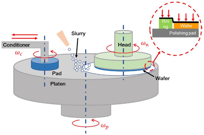
CMP (Chemical Mechanical Planarization) 공정은 반도체 생산 공정에서 웨이퍼의 국소 및 광역 평탄화를 위한 필수적인 기술로써, 연마패드와 웨이퍼의 직접 접촉에 의한 기계적 작용과 연마입자가 포함된 슬러리(Slurry)와 웨이퍼 박막 사이에서 발생하는 화학적인 작용을 통해 웨이퍼 표면의 결함과 요철을 제거한다(
Fig. 1). CMP 공정의 가장 이상적인 결과는 웨이퍼의 모든 위치에서 균일한 재료 제거율(Removal Rate)이 나타나는 것이지만, 다양한 원인에 의해 웨이퍼 가장자리에서 비정상적인 재료 제거율이 발생하게 되고, 이러한 현상을 지칭하는 에지 효과(Edge Effect)에 의해 반도체 소자 생산이 불가능한 영역이 형성된다. 웨이퍼의 직경이 커질수록 한 장의 웨이퍼로부터 생산 가능한 소자의 개수는 증가하며, 경제적인 효율도 증가한다. 하지만 웨이퍼의 직경이 증가할수록 한 장의 웨이퍼에서 에지 영역이 차지하는 비율은 줄어들지만, 에지 영역의 절대적인 면적은 늘어난다.
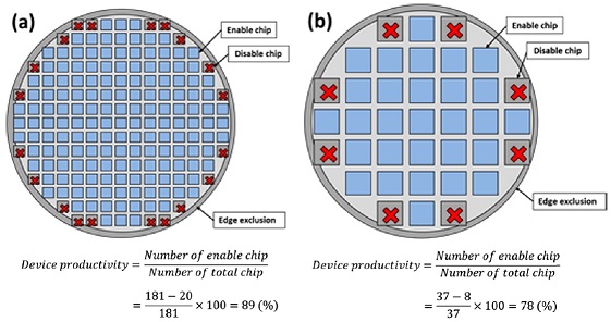
1 현재, 반도체 산업의 선도적인 업체들은 웨이퍼 에지 영역을 2-3 mm 이내로 유지하고 있는 상황이고, 1 mm 이내로 축소시키는 연구개발이 활발하게 진행 중에 있다. 에지 영역이 웨이퍼의 끝단에서부터 3 mm만 되어도 에지 영역에 포함되어 버려지는 반도체 소자의 수가 30%에 달하게 된다.
2 Fig. 2에서 알 수 있듯이 소자의 크기가 100 mm
2 이하인 모바일 어플리케이션 프로세서나 메모리보다 100-400 mm
2의 CPU (Central Processing Unit) 또는 GPU (Graphics Processing Unit)는 에지 영역의 크기가 하나의 웨이퍼에서 생산 가능한 소자의 생산성에 결정적인 영향을 주는 요소로 작용한다. 따라서, 웨이퍼 에지 영역에서 발생하는 재료 제거율의 경향 확인 및 에지 영역 재료 제거율의 균일화는 필수 불가결한 과제이다.
Fig. 1 Schematics of chemical mechanical planarization process

Fig. 2 Comparison example of device productivity by device size: (a) Mobile application processer, (b) CPU

이러한 과제를 해결하기 위해 CMP 헤드 내 구성 요소의 기하학적 치수 등을 최적화하여 균일한 에지 영역 재료 제거율을 얻으려는 연구가 진행되어 왔다. 하지만 균일한 재료 제거율 결과를 얻을 수 있는 적정 분할 치수를 찾기 위해서는 매번 다른 치수를 가진 부품을 제작하고 실험계획법에 바탕을 둔 반복 실험이 필요하며 이는 부품 제작 비용 및 시간, 반복 실험 등 많은 요구사항이 필요함을 의미한다. 이러한 기구실험을 대체하기위해 유한요소해석(Finite Element Analysis, FEA)을 도입하는 연구 또한 진행 중이다.
2-4 본 연구에서는 유한요소해석을 기반으로 하는 웨이퍼 에지 영역의 접촉응력 분포 시뮬레이션 모델을 제작하고 시뮬레이션 모델과 실제 CMP 공정 모델 간의 정합성을 선행적으로 확인하는 것을 목표로 하였다.
2. 실험방법
2.1 웨이퍼 접촉응력 유한요소해석
유한요소해석을 수행하기 위하여 필수적으로 정의되어야 할 요소는 해석 대상의 기하학적 치수, 구성 요소 별 재료 물성 값, 구성요소 간 접촉조건, 하중, 구속 등의 경계조건이 있다.
2.1.1 해석 대상의 기하학적 치수 정의
본 연구에서는 정적 상태에서 구조해석을 수행하였다. 해석 대상은 반도체 산업 양산 단계에서 가장 많이 사용되는 12인치 실리콘 웨이퍼로 설정하였다. 12인치 웨이퍼와 이를 연마할 수 있는 CMP 핵심 구성요소를 해석하고자 하였으며, 웨이퍼 에지 영역의 접촉응력 집중 만을 관찰하기 위하여 웨이퍼, 연마패드, 리테이닝 링을 제외한 나머지 구성요소는 경계조건화 하여 생략하였다. 해석 대상 중 리테이닝 링은 12인치 웨이퍼를 링 내부에 장착할 수 있도록 내경을 301 mm로 설정하였다. 연마패드는 경질 폴리우레탄(Polyurethane)의 그루브(Groove)가 없는 평면 패드로 정의하였으며 연마패드와 리테니어 링, 웨이퍼 간 완전히 밀착된 상태로 설정하였다. 해석 시간을 줄이기 위하여 대칭 조건을 부여하였다.
2.1.2 재료 물성 값 설정
유한요소해석을 위해 웨이퍼, 연마패드, 리테이닝 링에 대한 재료 물성치를 설정하였다. 선형 정적 해석에서 필요로 하는 재료 물성 값은 탄성계수와 푸아송 비로 대표된다. 웨이퍼와 리테이닝링의 경우 각각 실리콘, PEEK (Polyether Ether Ketone)로 제작되었으며 이에 대한 재료 물성 값을 해석 모델에 부여하였다. 연마패드는 웨이퍼나 리테이닝 링과 달리 점탄성(Viscoelasticity) 거동을 보이는 폴리우레탄이기 때문에 인장 실험을 통하여 직접적으로 탄성계수와 푸아송 비를 얻을 수는 없다. 따라서 동적기계분석(Dynamic Mechanical Analysis, DMA)을 통해 저장 계수(Storage Modulus,
E')와 손실 계수(Loss Modulus,
E')를 측정해야 하고 이를 선형 유한요소해석에 적용할 수 있게 변형하는 단계를 거쳐야 한다. Lu
5 등은 CMP 공정에서 주로 사용하는 연마패드의 점탄성 특성을 동적기계분석을 통하여 얻었다. 본 연구에서 대상으로 하는 경질 폴리우레탄 연마패드의 저장계수는 상온 25
oC 에서 약 400 MPa 로 나타난다. 또한 손실 계수와 저장 계수의 비로 표현되는 tanδ는 약 0.08으로 확인하였다. 정적 구조 해석에서 점탄성 재료의 탄성계수(E)는 선형 거동 범위 내에서 근사적으로
식(1)과
식(2)으로 표현이 되며 이를 통해 경질 폴리우레탄 연마패드의 탄성계수는 약 401 MPa로 표현할 수 있다.
연마패드의 푸아송 비는 대부분의 고분자 재료와 마찬가지로 이론상 최대치인 0.5에 근접한 값을 가진다.
6,7 본 연구에서는 경질 폴리우레탄 연마패드의 푸아송 비를 0.45로 설정하였으며 유한요소해석에 사용한 모든 재료 물성 값을
Table 1에 나타내었다.
Table 1Material properties of wafer, pad and retainer ring
Table 1
|
Parameter |
Conditions |
Young’s modulus
(MPa) |
Wafer |
160,000 |
|
Pad |
401 |
|
Retainer ring |
3,600 |
|
Poisson’s ratio |
Wafer |
0.3 |
|
Pad |
0.45 |
|
Retainer ring |
0.38 |
2.1.3 접촉 조건 및 경계 조건 설정
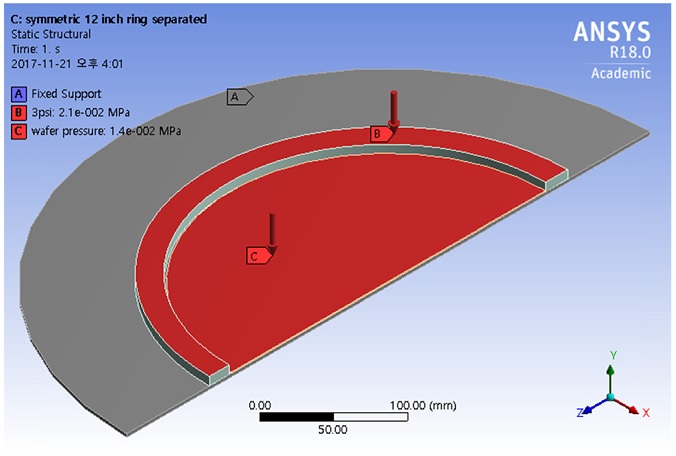
본 연구에서 유한요소해석을 수행하고자 하는 모델은 웨이퍼, 연마패드, 리테이닝 링으로 총 3개의 요소로 구성되어 있다. 이는 웨이퍼-연마패드, 연마패드-리테이닝 링, 리테이닝 링-웨이퍼 간의 접촉이 발생함을 의미하며 이들 간의 접촉 조건을 설정해주는 단계가 필수적이다. 패드 리바운드 현상이 발생했을 때, 패드의 상부면이 변형함에 따라 웨이퍼는 연마패드 상부면의 수직 방향으로 휠 것으로 예상되며 이를 반영하기 위해 웨이퍼와 연마패드의 계면이 분리 될 수 있는 자유도를 부여하였다. 경계 조건은
Fig. 3과 같이 정의하였다. 먼저 연마패드의 하부면에 고정 구속을 부여하였다. 웨이퍼의 상부면에 2 psi의 균일 압력을 부여하고 리테이닝 링의 상부면에 2 psi에서 10 psi까지 1 psi씩 압력을 증가시켰을 때, 웨이퍼 에지 영역에서 웨이퍼의 하부면이 받는 접촉응력 분포를 얻고자 하였으며 ANSYS Workbench 소프트웨어에서 경계 조건이 부여된 상태를
Fig. 4에서 확인할 수 있다.
Fig. 3Schematics of contact conditions and boundary conditions
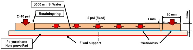
Fig. 4Schematics of contact conditions and boundary conditions in FEA software

2.2 웨이퍼 압력 측정
압력의 크기를 읽고 신호를 출력하는 압력 중 압전 소자형 센서는 압력이 가해 졌을 때 발생하는 변형량의 변화를 압전 효과를 이용하여 압력의 크기를 계산하는 방식이며, 정적인 상태에서 받는 압력과 비례하는 신호 출력을 보여준다. 또한 압력 센서의 크기를 초소형화 할 수 있으며 센서의 두께도 얇게 제작이 가능하기 때문에 0.5 mm의 두께를 가지는 고분자 시트에 수백개의 측정 포인트를 갖는 센서도 제작이 가능하다. 하지만 센서의 제조비용이 높으며 신호처리를 위한 별도의 단말기와 소프트웨어가 필수적이라는 단점이 있다. 본 연구에서는 Tekscan 사의 I-Scan System 압전 소자형 압력 센서를 사용하여 웨이퍼 에지 영역에서의 접촉 응력을 측정하고자 하였으며 압력 센서의 사양
8은
Table 2와 같다.
Table 2Specifications of I-Scan system pressure sensor
Table 2
|
Parameter |
Line type |
Plane type |
Dimension
(mm) |
Length |
400 |
44.7 |
|
Width |
10 |
44.7 |
|
Pitch |
Columns |
- |
1.0 |
|
Rows |
1.29 |
1.0 |
|
Quantity |
Columns |
- |
44 |
|
Rows |
350 |
44 |
Sensel spatial resolution
(sensel/cm2) |
96.9 |
Max pressure
(psi) |
50 |
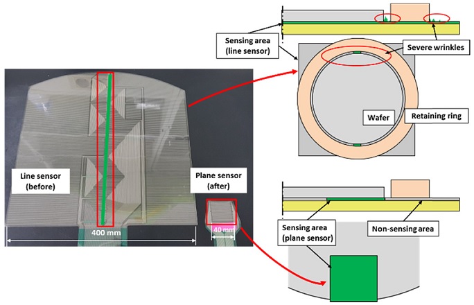
라인 센서는
Fig. 5와 같이 가로 400 mm, 세로 400 mm, 두께 0.5 mm의 치수를 가졌으며 이 크기는 12인치 웨이퍼 뿐만 아니라 12인치 캐리어에 장착되는 리테이닝 링의 외경보다도 큰 치수이다. 따라서 압력 센서를 웨이퍼-패드 사이에 위치한 상태에서 압력 조건을 부여하면 리테이닝 링과 웨이퍼 사이의 간격에 의한 공간 및 리테이닝 링 외부에서의 센서 시트 구겨짐이 크게 발생한다. 압력 센서 시트에 의도치 않은 추가 변형이 발생하면 인근 영역에 인장, 압축응력을 부여하게 되어 수직 방향으로의 압력 영향뿐 만 아니라 수평 방향으로의 응력 영향도 받게 되어 센서 측정 결과에 악영향을 미친다. 이와 달리 1개의 일렬 센서가 아닌가로 40 개 세로 40 개의 측정 포인트를 가진 면 센서는 라인 센서에 비해 10배 작은 치수를 가지고 있으며
Fig. 5와 같이 웨이퍼 에지 영역에만 위치할 수 있다. 또한 모든 측정 포인트는 완전히 웨이퍼 영역에만 위치하기 때문에 리테이닝 링에 의한 측정 포인트의 구겨짐 등이 발생하지 않으므로 본 연구에서는 면 센서를 사용하여 웨이퍼 에지 영역에서의 압력 측정을 수행하였다.
Fig. 5Comparison between type of pressure sensors
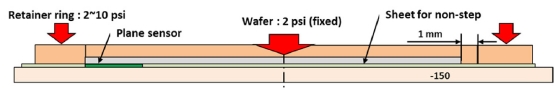
면 센서를 이용한 압력 측정 실험은
Fig. 6과 같이 구상하여 진행하였다. 먼저 웨이퍼가 패드와 맞닿는 표면에서의 압력을 측정하기 위하여 면 센서를 웨이퍼와 연마패드 사이에 배치하였다. 웨이퍼 에지 영역에만 면 센서의 측정 영역이 위치하도록 면 센서를 위치하였으며 사용한 면 센서는 두께 0.5 mm로 매우 얇은 편이지만 그 두께로 인해 면 센서의 가장자리에 압력이 집중되는 것을 막기 위하여 동일한 두께의 폴리머 시트를 면 센서 주위 영역에 배치하였다. 그 후 웨이퍼에 2 psi의 균일 압력을 부여한 상태에서 리테이닝 링에 2 psi에서 10 psi까지 1 psi 만큼씩 점차 압력을 증가하였을 때 면 센서의 압력 신호 크기를 웨이퍼 중심으로부터 141 mm부터 150 mm까지 총 10 개의 측정 포인트에서 얻었다.
Fig. 6Schematics of pressure measurement in wafer edge area using plane sensor sheet

3. 장 실험결과 및 고찰
3.1 유한요소해석 접촉응력 분포
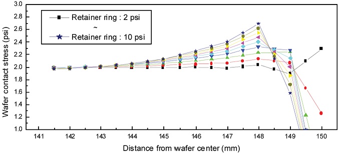
Fig. 7은 유한요소해석을 통해 얻은 웨이퍼 에지 영역의 접촉응력 분포도이다. 웨이퍼 중심으로부터 141-150 mm 내의 범위에서 접촉응력의 분포를 도시하였다. 접촉응력 분포를 보았을 때 리테이닝 링에 인가된 압력이 증가할수록 웨이퍼 반경 148 mm지점에서 접촉응력 크기가 증가하는 것을 확인하였다. 또한 웨이퍼 중심 영역에서 나타나는 접촉응력 대비 최대 1.3배 큰 값을 보여준다. 이러한 결과는 기존 연구에서도 확인이 가능한 결과이며 본 연구에서 제작한 유한요소해석 모델이 웨이퍼 에지 효과를 보여줌을 의미한다.
Fig. 7Distribution of wafer contact stress in edge area by FEA

3.2 웨이퍼 에지 영역 압력 측정
유한요소해석으로 얻은 접촉응력은 압력 단위로 표현되는 반면 압력 센서의 신호 크기는 무차원의 단위를 가지기 때문에 상호 비교를 위하여 추가적인 조정 실험을 수행하였다.
Fig. 8과 같이 웨이퍼 중심 영역에 면 센서를 배치하고 웨이퍼의 상부면에 1 psi의 압력을 부여하고 1 psi씩 압력을 증가시켰을 때 센서에서 출력되는 신호의 크기를 확인하였다.
Fig. 9는 웨이퍼 인가압력 변화에 따른 센서 신호크기 변화를 도시한 그래프이며 인가압력과 센서 신호 크기 간 약 99%의 높은 상관관계를 가짐을 알 수 있었다. 이를 바탕으로 무차원 단위의 센서 신호 크기를 압력 단위로 변환할 수 있는 단위 변환식을 얻었다.
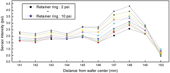
Fig. 10은 압전 소자형 압력 센서를 사용하여 웨이퍼 에지 영역의 압력을 측정한 결과에
Fig. 8의 측정을 통해 얻은 변환식으로 센서 신호 크기를 압력 단위로 변환한 그래프이다. 유한요소해석으로 얻은 접촉응력 분포도와 마찬가지로 웨이퍼 중심으로부터 141-150 mm 영역 내의 압력 센서 신호 크기를 1 mm 간격으로 도시하였다. 리테이닝 링에 인가한 압력이 증가할수록 웨이퍼 반경 148 mm 지점에서 센서의 신호 크기가 가장 높게 나타남을 확인하였으며, 리테이닝 링에 점점 더 높은 압력을 부여할수록 센서 신호 크기도 비례하여 증가하는 경향을 보였다.
Fig. 8Schematics of pressure measurement for convert units
Fig. 9Correlation between wafer input pressure and sensor output intensity
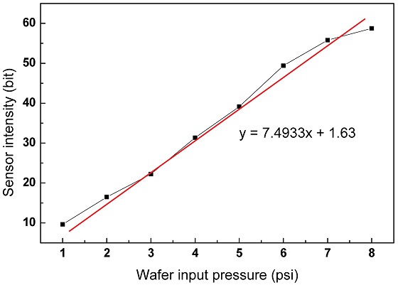
Fig. 10Result of pressure measurement after converting unit

3.3 접촉응력과 측정압력의 정합성 비교
압전 소자형 면 센서로 측정한 압력신호 분포(
Fig. 10)와 수정된 유한요소해석 모델을 이용하여 얻은 접촉응력 분포(
Fig. 7)를 비교하여 실제 압력분포 대비 해석 상의 접촉응력 분포 경향이 어느 정도 유사한지를 확인하였다.
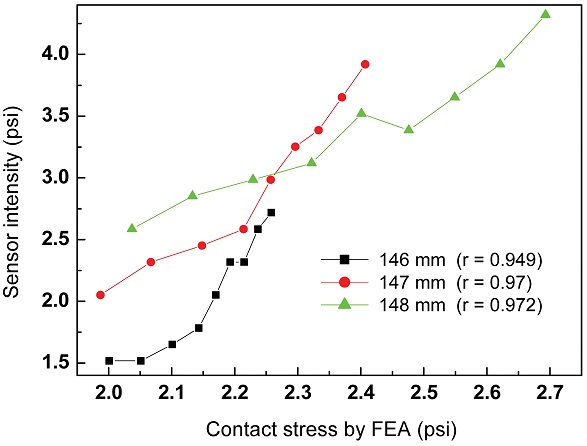
Fig. 11은 웨이퍼 에지 영역에서도 주요 관심 영역인 웨이퍼 반경 146-148 mm 내의 데이터들을 상호 비교한 결과 그래프이다. 각 지점에서 접촉 응력과 압력 센서의 신호 간 상관계수(Correlation Coefficient,
r)는 0.94-0.97의 범위 내에서 높게 나옴을 확인하였다. 이를 통해 본 연구에서 제작하고 수정한 유한요소해석 모델이 실제 CMP 헤드 내에서 웨이퍼 에지 영역에서 웨이퍼-연마 패드-리테이닝 링의 거동을 94-97% 정도로 유사하게 보여줌을 증명하였다.
Fig. 11Correlation between results of FEA and measurement at 146 mm, 147 mm and 148 mm

4. 결론
CMP 공정에서 연마패드의 리바운드 현상을 주 원인으로 하여 웨이퍼 에지 영역에서 재료 제거율이 불균일하게 나타난다. 본 연구에서는 CMP 공정에서 웨이퍼 에지 영역에서 발생하는 응력 집중 현상을 유한요소해석 상으로 확인하고 개선할 수 있는 시뮬레이션 모델을 제작하고 압력 센서의 측정 결과와 일치하는지를 확인하고자 하였다. 먼저 선행 연구 등을 참고하여 유한요소해석에 적용할 재료 물성치와 경계조건, 접촉조건 등을 설정하였다. 제작한 유한요소해석 모델을 사용하여 웨이퍼 에지 영역에서의 접촉응력 분포를 계산하였으며 그 결과 공학적으로 유의미한 웨이퍼 에지 접촉응력 분포 프로파일을 얻었다. 다음으로 압전 소자가 내장된 면 타입의 압력 센서을 사용하여 웨이퍼 에지 영역에서 발생하는 압력을 측정하였다. 측정한 압력 센서 신호는 유한요소해석 결과인 접촉응력과 비교하기 위하여 무차원의 센서신호단위에서 압력 단위로 변환하는 과정을 거쳤다. 마지막으로 유한요소해석 모델의 접촉응력 분포와 상관관계를 비교하여 유한요소해석 모델이 실제 웨이퍼 에지 영역 압력 분포 경향과 유사한 결과를 보이는지 확인하였다. 그 결과 웨이퍼 반경 145-148 mm내에서 유한요소해석 결과와 실제 압력 측정 결과의 경향이 90% 이상 일치함을 확인하였다. 이를 통해 본 연구에서 제작 및 수정한 유한요소해석 시뮬레이션 모델이 CMP 장비 내 구성요소의 실제 거동 경향과 정합성이 있음을 증명하였다.
본 연구를 통해 제작된 유한요소해석 모델은 웨이퍼 중심 영역 대비 에지 영역에서 크게 발생하는 접촉응력을 줄이기 위한 연구에 활용할 수 있다. 특히 CMP 헤드에 장착하는 리테이닝 링의 폭, 웨이퍼와의 간격을 결정하는 내경 등을 최적화하는 데에 기여할 수 있다고 판단한다.
ACKNOWLEDGMENTS
이 연구은 2016년도 정부(미래창조 과학부)의 재원으로 한국연구재단의 지원을 받아 수행된 연구임(No. 2016R1A2B4011466).
REFERENCES
- 1.
Tönshoff, H., Schmieden, W. V., Inasaki, I., König, W., and Spur, G., “Abrasive Machining of Silicon,” CIRP Annals-Manufacturing Technology, Vol. 39, No. 2, pp. 621-635, 1990.
10.1016/S0007-8506(07)62999-0
- 2.
Eamkajornsiri, S., Narayanaswami, R., and Chandra, A., “Yield Improvement in Wafer Planarization: Modeling and Simulation,” Journal of Manufacturing Systems, Vol. 22, No. 3, pp. 239-247, 2003.
10.1016/S0278-6125(03)90023-9
- 3.
Wang, T., Lu, X., Zhao, D., and He, Y., “Contact Stress Non-Uniformity of Wafer Surface for Multi-Zone Chemical Mechanical Polishing Process,” Science China Technological Sciences, Vol. 56, No. 8, pp. 1974-1979, 2013.
10.1007/s11431-013-5245-y
- 4.
Chen, K.-S., Yeh, H.-M., Yan, J.-L., and Chen, Y.-T., “Finite-Element Analysis on Wafer-Level CMP Contact Stress: Reinvestigated Issues and the Effects of Selected Process Parameters,” International Journal of Advanced Manufacturing Technology, Vol. 42, No. 11, pp. 1118-1130, 2009.
10.1007/s00170-008-1672-5
- 5.
Lu, H., Obeng, Y., and Richardson, K., “Applicability of Dynamic Mechanical Analysis for CMP Polyurethane Pad Studies,” Materials Characterization, Vol. 49, No. 2, pp. 177-186, 2002.
10.1016/S1044-5803(03)00004-4
- 6.
Mott, P., Dorgan, J., and Roland, C., “The Bulk Modulus and Poisson's Ratio of “Incompressible” Materials,” Journal of Sound and Vibration, Vol. 312, No. 4, pp. 572-575, 2008.
10.1016/j.jsv.2008.01.026
- 7.
Luo, J. and Dornfeld, D. A., “Integrated Modeling of Chemical Mechanical Planarization for Sub-Micron IC Fabrication: From Particle Scale to Feature, Die and Wafer Scales,” Springer Science & Business Media, pp. 62-63, 2013.
- 8.
Citations
Citations to this article as recorded by

- Multi-objective Optimization of CMP Retainer Ring based on a Metamodel Approach
Do Yeong Jung, Seung Heon Lee, Jae Phil Boo, Jung Woo Lee, Byung Wan Kim, Gu Young Cho
Journal of the Korean Society for Precision Engineering.2026; 43(6): 605. CrossRef - FEM Studies of CMP Retainer Ring Using Metamodel
Do Yeong Jung, Seung Heon Lee, Jun Geon Park, Jae Phil Boo, Jung Woo Lee, Byoung Wan Kim, Gu Young Cho
Journal of the Korean Society for Precision Engineering.2025; 42(12): 1065. CrossRef - Variation of Pad Temperature Distribution by Slurry Supply Conditions
Jinuk Choi, Seonho Jeong, Kyeongwoo Jeong, Haedo Jeong
Journal of the Korean Society for Precision Engineering.2020; 37(12): 873. CrossRef