ABSTRACT
Energy beam machining is a type of micro/nano-manufacturing technology for advanced materials. The energy beam is composed of the matter which exhibits not only particle but also wave-like behaviors. In this paper, we focused on the energy beam machining using the charged particles, which is classified into electron beam and ion beam machining. The equipment and principles of irradiation of electron beam and ion beam are investigated, and the range of technologies according to the energy beam characteristics is summarized. For the electron beam machining, recent studies for equipment development of surface heat treatment process and electron beam melting process using low-power electron beam are summarized. For the ion beam machining, recent studies on focused ion beam machining with various materials, such as high hardness materials, optical materials and semiconductor materials, are summarized. The studies for improving the accuracy and productivity of focused ion beam machining was is summarized. It was found that numerous technologies using the energy beam have been achieved for manufacturing of micro/nano-components with high precision. It is expected that the energy beam machining becomes a promising manufacturing technology for advanced materials.
-
KEYWORDS: Micro/nano manufacturing, Low-power electron beam process, Focused ion beam machining, Nanofabrication
-
KEYWORDS: 마이크로/나노 생산, 저출력 전자 빔 공정, 집속이온빔 가공, 나노제작
1. 서론
최근 항공 우주, 자동차, 의료 등의 다양한 분야에서 신소재를 이용한 부품이 개발되면서 에너지 빔 가공 기술에 대한 수요가 증가하고 있다.
1-3 에너지 빔 가공 기술은 전통적인 기계가공 기술과 달리 공구로 사용되는 빔이 마모가 일어나지 않기 때문에 안정적이고 정밀한 가공이 가능하다. 또한, 금속뿐만 아니라 세라믹, 복합, 바이오 소재 등 전통적인 기계가공의 제한이 있는 소재에도 적용이 가능하기 때문에 첨단 신소재 기반 초미세 부품을 가공할 수 있는 기술로 주목 받고 있다.
에너지 빔 가공 기술은 입자와 파동의 특징을 가진 물질을 빔의 형태의 운동에너지를 가지며, 시료 표면의 물리적, 화학적 특성을 변형시키는 기술이다. 대표적으로 광자를 이용한 레이저 가공 기술이 있으며,
4 하전 입자를 이용한 전자 및 이온 빔 가공 기술도 에너지 빔 가공 기술로 분류된다.
5,6 이 기술들은 빔 입자의 운동에너지가 시료 표면에 전달되어 열에너지 또는 운동에너지로 변환되는 현상을 이용한다. 예를 들어, 레이저 빔 또는 전자 빔의 경우, 빔 에너지가 시료 표면에서 열에너지로 변환되고 변환된 열에너지에 의해 시료 표면에 용융 또는 증발 현상이 발생한다. 이온 빔의 경우, 빔 에너지가 시료 표면에서 운동 에너지로 변환되어 빔이 조사된 영역 내부의 원자들의 연쇄 충돌을 야기한다. 변환된 에너지에 의해 시료 표면의 원자들은 증발 또는 탄성충돌에 의해 제거되거나 용융 또는 비탄성 충돌에 의해 재배열된다. 이처럼 에너지 빔 가공 기술은 시료의 표면을 원자 레벨의 미세 영역에서 물리적, 화학적 특성을 변형시킬 수 있기 때문에 마이크로/나노 단위의 미세 가공 기술로 활용되고 있다.
7,8
이 논문에서는 에너지 빔 가공 기술 중에서도 전자 빔 가공 기술과 이온 빔 가공 기술에 대한 소개를 하고자 한다. 전자 빔(Electron Beam, EB)은 미세 구조를 관측하는 현미경인 주사 전자 현미경(Secondary Electron Microscope, SEM)와 투과 전자현미경(Transmission Electron Microscope, TEM)에 주로 쓰였다. 최근에는 높은 에너지의 전자 빔 장치가 개발되면서 밀링, 드릴링, 용융, 적층, 표면 처리 등의 다양한 공정에 활용되고 있다. 전자 빔은 높은 열에너지 전환 효율을 가지기 때문에 레이저 가공의 대체 기술로 주목 받고 있다. 마찬가지로 이온 빔 기술은 시료 표면의 미세 구조를 관측하는 용도 뿐만 아니라 표면에 미세 패턴을 가공하는 용도로도 사용되고 있다. 이온 빔을 이용한 가공 가술은 반도체, 전자, 통신, 광학 등의 여러 분야에서 요구되는 수 nm급 고정밀 부품 제작 및 프로토타이핑에 활용되고 있다.
이 논문의 2절은 전자 빔 장비 및 가공 원리에 대해 소개하였고, 저출력 전자 빔을 이용한 표면 열처리 공정과 메탈 적층 공정 관련 연구에 대해 정리하였다. 3절은 초미세 가공 공정에 주로 사용되는 집속 이온 빔(Focused Ion Beam, FIB)의 장비 및 가공 원리에 대해 소개하였고, FIB를 이용한 초미세 소자 제작 연구들을 가공 대상 재료에 따라 정리하였으며, 가공 정밀도 및 생산성 향상 관련 연구를 소개하였다. 마지막으로, 4절 결론과 함께 논문을 마무리하였다.
2. 전자 빔 응용 가공 기술
2.1 전자 빔 장비 및 가공 원리
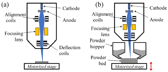
전자 빔 장치의 기본적인 원리를 설명하기 위해 전자 빔 장치의 구성을
Fig. 1(a)에 도시하였다. 음극(Cathode)은 전자를 방출하는 전자 원(Electron Source)이다. 방출된 전자는 전자기 코일(Alignment Coils)을 지나며 빔 축에 정렬되고, 전자기장 렌즈(Focusing Lens)를 통해 집속되어 에너지 밀도가 증가된 빔의 형태가 된다. 그리고 편향 코일(Deflection Coils)에 의해 진행 방향이 제어된다.
Fig. 1Schematic of the basic component of the EB system for (a) drilling, melting, welding, or surface treatment and (b) 3D printing processes

전자 원에서 방출된 전자는 전하와 질량을 가진 입자로 가속 장치에서 가속되어 운동 에너지를 가지게 되며, 소재 내부의 전자(자유전자와 속박전자), 양성자와 정전기적 상호작용을 통해 소재의 열 에너지로 전환되는 메커니즘을 가진다. 전자 빔 가공 공정은 기본적으로 전자 빔의 운동 에너지가 재료의 열 에너지로 변환되면서 발생하는 재료의 상변화(고체-액체-기체)를 유도하는 가공방식이다. 따라서 현재 전자 빔 가공(열 처리, 메탈 적층, 드릴링 공정 등)의 주요 가공 파라미터는 상변화 관련 물성치(열 전도도, 비중, 열 팽창률, 용융 온도 등)와 전자 빔 관련된 파라미터(가속전압, 전류, 빔 직경, 작업거리 등)가 있으며, 이들 파라미터가 기계적 물성치, 재료적인 마이크로 구조 변화에 미치는 영향에 대한 연구 등이 활발히 수행되고 있다.
Fig. 1(b)는 PBF (Power Bed Fusion) 전자 빔 메탈 적층 가공에 사용되는 전자 빔 장치의 기본 구성이다. 분말 형태의 재료를 공급하는 부분이 있으며,
Figs. 1(a)와
1(b) 모두 편향 코일의 위치가 집속 전자기장 렌즈보다 하부에 있는 특징이 일반적인 SEM과 다른 점이다.
전자 원은 음극의 종류에 따라 열 음극 전자 원(Thermionic Cathode Electron Source)과 냉 음극 전자 원(Cold Cathode Electron Source)으로 구분된다.
Fig. 2는 열 음극 전자 원과 냉음극 전자 원의 전자 방출 메커니즘을 보여준다. 일반적으로 전자 빔 장비들은 열 전자 원을 사용한다.
9
Fig. 2Electron emission mechanism of the electron beam accelerator with (a) a thermionic hot cathode and (b) a plasma cold cathode13
열 음극 전자 원은
Fig. 2(a)와 같이 필라멘트의 자유전자가 일함수 이상의 에너지로 가열되었을 때 음극 내부의 자유전자를 방출시킨다. 일반적으로 필라멘트 소재는 텅스텐으로, 텅스텐이 2200
oC 이상의 온도에서도 기계적 및 화학적 안정도를 가지는 소재이기 때문이다.
10 토륨(Thorium) 또는 산화물이 추가된 텅스텐 필라멘트가 사용되기도 하는데, 불순물이 첨가된 텅스텐은 일함수가 낮아져 전자 빔 방출 효율이 높기 때문이다. 하지만, 이들 열전자 원은 화학적 반응에 의한 필라멘트 수명에 좋지 않고 특히, 진공 유지가 까다로운 단점이 있다. 열 음극 방식을 이용한 전자 빔 가공에는 가공 소재의 기화(Vaporization)에 의한 진공도 감소와 2200
oC 이상의 고온 상태의 전자 빔 방출 시 텅스텐 필라멘트 소재 내부의 마이크로 구조변화(Grain Growth, Recrystallization, Oxidation 등)가 필라멘트 수명을 매우 짧게 만드는 단점이 있다. 이를 극복하기 위해, 플라즈마 방식의 냉 음극 전자 원을 이용한 전자 빔 방출 및 가속 장치에 대한 연구가 활발히 이루어 지고 있다.
11-14
냉 음극 전자 원은 플라즈마 에너지를 직접 또는 간접적인 방법으로 이용하여 음극 내부의 자유 전자를 방출시킨다.
Fig. 2(b)는 플라즈마의 중성입자와 양이온에 의한 플라즈마 에너지의 간접적인 전자 빔 방출원리를 나타낸다.
13 Fig. 3은 세가지 방식의 플라즈마 에너지를 이용한 냉 음극의 전자 빔 방출 및 가속 방식을 도식하고 있다.
Figs. 3(a)-
3(c)는 각각 비정상 글로우 방전(Abnormal Glow Discharge) 기반 플라즈마 다이오드 음극, 정상 글로우 방전(Normal Glow Discharge) 기반 플라즈마 공 음극, 아크 방전(Arc Discharge) 기반 플라즈마 폭발 음극 방식의 예시를 나타낸다.
Fig. 3Typical types of the electron beam accelerator with the plasma cold cathode: (a) Plasma diode cathode, (b) Plasma hollow cathode, (c) Plasma explosive cathode13
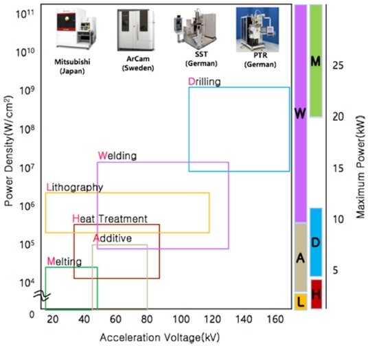
전자 빔 장치는 가속 전압, 파워 밀도, 최대출력 등의 빔 특성에 따라 그 응용 범위가 구분되는데, 이를
Fig. 4에 도시하였다.
13
Fig. 4Specifications of power, power density and acceleration voltage for an electron beam process13

먼저, 저 출력의 전자 빔을 이용한 공정으로는 표면 열 처리 공정(Heat Treatment)과 메탈 적층 공정(Additive)이 있다. 전자 빔을 이용한 표면 처리 공정은 주로 표면에만 열을 주입하기 때문에 10
5W/cm
2의 파워밀도, 5 kW급의 낮은 출력을 필요로 한다.
15-18 최근 활발히 연구되고 있는 전자 빔 메탈 적층 공정도 열 처리 공정과 유사하게 표면의 0.5 mm이내 깊이만 용융하기 때문에 60 kV 급의 가속 전압과 5 kW급 이하의 낮은 출력이 요구된다.
19-21
반면, 고 출력의 전자 빔을 이용한 공정으로는 용융(Melting), 용접(Welding) 및 드릴링(Drilling)이 있다. 이러한 고출력 공정의 경우 20 kW이상의 큰 출력이 요구되는 반면 용융공정의 파워밀도는 10
4W/cm
2 용접공정은 10
6W/cm
2, 드릴링 공정은 10
7W/cm
2 정도로 응용 분야별로 차이가 난다. 10 kW이상의 높은 출력의 전자 빔 용접 공정의 가장 큰 장점으로는 깊고 정밀한 용접이 가능하다는 점이며, 연구 결과에서 30-100 mm의 균일한 용접 깊이가 보고되고 있다.
22,23 그 밖의 공정으로는 전자 빔을 이용한 드릴링(Drilling) 공정이 있다. 세장비 10 이상, 직경 50 μm 이하의 미세홀 가공이 가능하며, 초당 2000 홀 이상의 가공 속도로 가공 시에도 홀 내부의 표면 조도가 낮고, 입/출구 부에 버가 거의 발생하지 않는 장점을 가진 것으로 보고되고 있다.
24
2.2절과 2.3절에서는 저 출력의 전자 빔을 이용한 공정인 표면 열처리 공정과 메탈 적층 공정 기술에 대해 소개하였으며, 특히 냉 음극 전자 빔인 플라즈마 전자 빔을 이용한 가공 연구에 대해 정리하였다.
2.2 전자 빔 응용 표면 처리 공정
전자 빔 표면 처리 공정은 표면의 경도 및 내부식성 향상, 표면조도를 개선하기 위한 기술로, 레이저 표면 처리 기술에 대응하는 정밀 기술로 주목 받고 있다. 표면 열처리에 사용되는 장비는 주로 열 음극 전자 빔 방식의 용접 장비이다. 따라서, 대부분의 주요 전자 빔 용접기 제조사의 경우 표면 열처리 공정이 용접 후나 단독 공정으로 이용된다.
25 하지만, 상용 장비는 열 전자 빔 원을 사용하기 때문에, 수명이 짧고 전자 빔 열처리 공정을 목적으로만 사용하기에는 고가인 단점이 있다. 이를 극복하기 위해 최근에는 플라즈마 에너지를 이용한 냉 음극 방출 및 가속기술을 적용하여 40 kV 이하의 낮은 가속전압 및 출력을 가지는 전자 빔 장비를 개발하려는 노력이 있다.
5,16-18 전자 빔 표면 처리 장치로 활용되기 위해서는 다른 공정에 비해 상대적으로 낮은 출력의 전자 빔을 방출하는 장비가 필요하다.
플라즈마 방식의 전자 빔은 열 전자 빔에 비해 전자 빔 원의 수명이 길고, 공정에 요구되는 파워밀도가
Fig. 4에 나타낸 바와 같이 10
5 W/cm
2 이하면 가능하다. 따라서, 저가화가 가능한 장점이 있다.
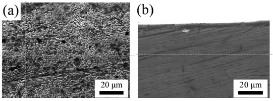
13 한국생산기술원(KITECH)은 낮은 파워밀도의 플라즈마 방식의 전자 빔 장비를 개발하는 연구를 수행하고 있다. KITECH에서 개발 중인 플라즈마 전자 빔 열처리 장비는 40-50 kV의 가속전압, 100 mA의 전류의 전자 빔을 방출할 수 있다.
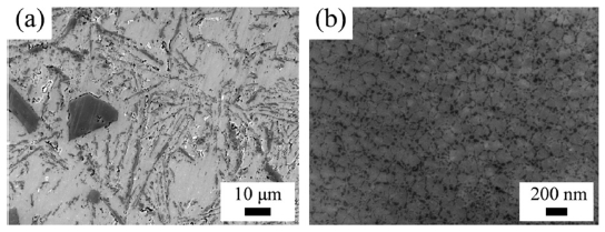
Fig. 5는 개발된 전자 빔 장비를 이용하여, 공구강 SK3의 표면처리의 전 후 이미지를 보여준다. 개발된 전자 빔 장비를 이용하여 처리된 탄소강 시료의 표면은 고크롬 탄화물(Cr Riched Carbide)의 제거 특성과 내부식성이 개선되었음이 보고되었다.
26,27
Fig. 5SEM images of cross-section of SK3 (a) before EB surface treatment and (b) after EB surface treatment

최근 나노 급 표면 처리 기술로 아크 방전 기반 플라즈마 폭발음극 방식의 전자 빔 기술에 대한 연구가 활발히 진행되고 있다. 이러한 아크형 전자 빔의 경우 30 mm 이상의 빔 크기로 시료의 가열, 용융, 증발, 응고 현상의 빠른 공정을 수행하기 때문에, 미세한 두께의 균일하고 빠른 표면 처리가 가능하다. 표면 처리 공정 이후 재료 표면은 마이크로 구조변화(Martensite, Carbide 등), 기화 온도가 낮은 소재(P, S 등)의 증발, 표면의 결함 감소 및 표면 조도 감소 등의 원인으로 물리적, 화학적 특성이 개선된다.
Fig. 6은 Al-15Si 시료의 표면을 플라즈마 폭발 음극 방식의 전자 빔으로 열 처리하기 전과 후의 SEM 이미지를 나타낸다. 초기 표면에서는 수십 μm의 크기를 갖는 작은 수의 Si상이 표면에 무작위로 분포된 과공정(Hypereutectic) 미세구조가 관찰되었다. 반면, 시료 표면은 마이크로 단위의 공융 구조가 감소하고, 5-50 nm크기의 나노 입자들이 표면에 균일하게 분포되었음이 확인되었다.
28
Fig. 6SEM images of hypereutectic Al-15Si (a) before and (b) after plasma explosive irradiation heat treatment28 (Adapted from Ref. 28 on the basis of open access)
그 밖에도 플라즈마 폭발 음극 기술은 텅스텐 합금소재,
29,30 크롬 합금소재,
31 40CrNiMo7,
32 스테인리스 강
33 등의 철강소재, 몰리브덴
34 등의 다양한 소재에 적용한 연구가 보고되고 있다. 이들 연구에서 플라즈마 폭발 음극 방식의 전자 빔으로 열 처리된 표면은 전자 빔의 펄스 수에 따라 미소 경도, 마모율, 내부식성 등의 특성이 향상되는 결과가 보고되었다.
전자 빔 응용 적층 기술은 EBM (Electron Beam melting) 또는 EBAM (Electron Beam Additive Manufacturing)로 불린다.
Fig. 1(b)와 같이 분말 소재를 분말 베드(Powder Bed)에 균일하게 분포시킨 후, 전자 빔을 조사하여 소결 및 용융 시켜 3차원 부품을 제작하는 기술이다.
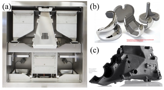
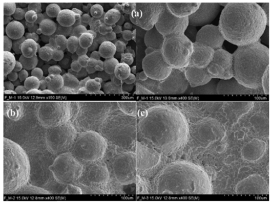
Fig. 7은 열 전자 빔 원을 이용한 전자 빔 장비(Arcam Q10plus, Arcam, 스웨덴)와 이 장비로 제작된 부품들의 대표 사진이다.
35 이 장비는 열 음극 방식을 이용한 전자 빔을 사용하며, 가속전압은 60 kV, 출력은 3 kW급이다. Ti6Al4V, Ti6Al4V ELI, Ti Grade 2, Arcam ASTM F75 Cobalt-Chrome, Alloy 718 소재를 대상으로 적층 공정을 수행한다. 이처럼 전자 빔 적층 연구는 주로 금속소재에 대한 적용연구가 수행되고 있다. 레이저를 이용한 메탈 적층 공정(Selective Laser Melting, SLM)과 비교하여, EBM으로 제작된 부품은 추가적인 열처리 공정을 수행하지 않고도, 충분히 안정적인 기계적 특성을 얻을 수 있다는 연구결과가 보고되고 있다.
36-38 또한, EBM 공정 시 고온(700-830
oC) 예열 처리가 미세 서브 그레인 구조 변화에 미치는 영향에 대한 연구도 보고되었다. 특히 고온 예열은 온도 및 응력 편차를 감소시켜 기계적 강도와 결함 감소에 효과가 있음이 보고되었다.
37,39
Fig. 7Photograph of (a) EBM machine with the thermionic hot cathode (Arcam, Sweden), (b) Femoral knee components and tibia trays, (c) Race car gearbox manufactured with Arcam EBM35 (Adapted from Ref. 35 on the basis of open access)

최근 비정상 글로우 방전 기반 플라즈마 다이오드 음극을 이용한 최대 출력 5 kW의 전자 빔 적층 공정 연구가 보고되었다.
40,41 냉 음극 전자 빔 원을 가진 장치이기 때문에 열 음극 전자 빔 원을 이용하는 상용 장비들에 비해 빔 수명이 길고, 저가로 생산할 수 있다는 장점을 가진다. 개발된 전자 빔 장치으로 Stellite21 분말의 적층 공정을 수행한 결과,
Fig. 8과 같이 전자 빔 출력에 따라 분말 비산 특성이 다름을 확인하였다. 이처럼 EBM 적층 공정 시 빔 조건에 따라 적층 된 부품의 마이크로 구조특성이 변화하고, 이는 제품의 수명에도 영향을 미친다.
21
Fig. 8SEM morphologies of the deposited beads by EBM with different acceleration voltages of (a) 12 keV, (b) 14 keV, and (c) 15 keV41 (Adapted from Ref. 41 with permission)
Ti-6Al-4V는 항공 우주 공학부터 의학까지 다양한 분야에서 사용되는 티타늄 합금 소재로 분말을 이용한 EBAM을 이용한 제조 공정이 연구되고 있다.
42-44 또한, 임플란트 소재로 쓰이는 순수 티타늄(CP-Titanium)을 EBAM으로 적층하는 연구도 진행되었다. CP-티타늄 소재의 경우 EBAM으로 적층한 구조물의 다공성에 따라 탄성 계수와 항복 응력이 결정됨이 보고되었다.
20 그 밖에도 316L 스테인리스강(Stainless Steel),
39 IN718 브라켓(Bracket)
45와 같이 다양한 소재의 부품을 제조하는데 EBM을 응용하려는 노력이 계속되고 있다.
3. 이온 빔 응용 미세 가공기술
3.1 집속 이온 빔 장비 및 가공 원리
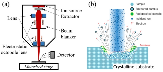
집속 이온 빔(FIB) 장치의 기본적인 원리를 설명하기 위해 FIB 장치의 구성을
Fig. 9(a)에 도시하였다. 이온 원(Ion Source)에서 만들어진 하전 입자(Charged Particles)는 추출기(Extractor)를 통과하며 가속되고, 정전기 8중극 렌즈(Electrostatic Octopole Lens) 등의 여러 렌즈들을 통과하며 집중되어 빔의 형태로 시료 표면에 조사된다. 이온 원은 액체 금속 이온 원(Liquid Metal Ion Source, LMIS)인 갈륨(Ga
+) 이온 원과, 가스장 이온 원(Gas Field Ion Source, GFIS)인 네온(Ne
+) 또는 헬륨(He
+) 이온 원 등이 있다. 이온 빔이 입사된 시료 표면에서는 원자뿐만 아니라 이차 전자(Secondary Electron, SE), 후방 산란 전자(Backscattered Electrons, BSE), 이차 이온(Secondary Ion, SI) 등이 방출된다. FIB 시스템은 방출된 입자들을 검출기(Detector)로 수집하여 가공 표면의 이미지를 제공한다. 여러 종류의 검출기를 동시에 설치할 수 있고, 검출기 종류에 따라 이차 전자 이미지,
46 전자 후방산란 회절 이미지,
47 X선 분광분석 이미지,
48 이차이온 질량분석 깊이 분포도
49 등을 동시에 측정할 수 있다. 즉, FIB 시스템은 고 에너지 이온 빔을 시료에 조사하여 표면의 특성을 변형시키는 동시에 변형된 표면의 이미지를 실시간으로 제공한다는 장점을 가진다.
Fig. 9Schematic of (a) typical type of FIB system and (b) ion beam irradiation on the crystalline substrate

시료 표면에 조사된 고 에너지의 이온 빔은 시료 표면의 형태 또는 원자 배열을 변형시킨다.
50 높은 에너지의 이온이 시료에 도달하면
Fig. 9(b)와 같이 입사된 이온과 표면 원자들의 연쇄 충돌(Collision Cascade)이 일어난다. 연쇄 충돌이 일어나는 영역에서는 탄성 혹은 비 탄성 충돌에 의해 재료 특성이 변형된다. 빔 에너지가 표면 원자의 결합에너지보다 높은 경우, 이온이 표면의 원자 결합을 끊어내고 원자를 외부로 방출시키는 스퍼터링(Sputtering) 현상이 일어난다. 반면, 이온 에너지가 표면 원자의 결합 에너지보다 낮은 경우, 이온이 표면의 원자와 연쇄 충돌하며 남아있게 되는 이온주입이 발생한다. 이에 따라 결정질의 구조였던 초기 시료 표면이 비정질 구조로 변형된다.
50
이처럼 입사 이온과 시료 내부의 입자가 이온-고체 상호작용(Ion-Solid Interaction)에 의해 재배열이 일어나는 영역을 이온 범위(Ion Range)로 정량화할 수 있다.
51 이온 범위는 빔 에너지가 같을 경우 이온 원에 따라서도 차이를 갖는다.
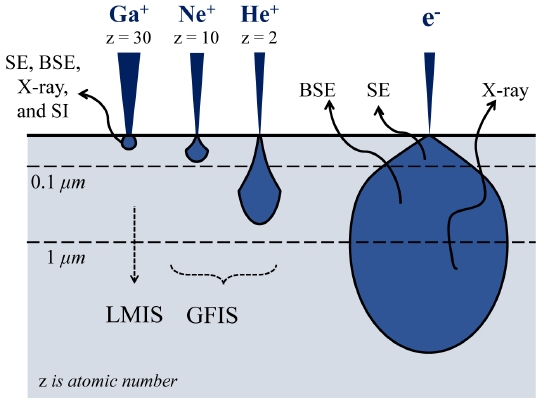
Fig. 10은 LMIS, GFIS, 전자(e
-)가 각각 같은 에너지로 시료에 조사되는 경우 이온 범위를 비교한 그림이다. 그림과 같이 LMIS와 GFIS는 전자 빔에 비해 표면 가까이에서 연쇄 충돌을 일으킨다. LMIS FIB와 GFIS FIB는 표면 가까이에서 이차입자(SE, BSE, X-ray, SI)를 발생시켜 표면에 매우 민감한 이미지를 생성할 수 있다.
52,53 또한, GFIS는 질량이 가벼워 이온 빔 조사 시 표면 손상이 거의 없다. 이에 따라 GFIS FIB는 금속뿐만 아니라 세라믹, 바이오 소재 등을 측정하는 현미경으로 활용되고 있다.
54
Fig. 10Modeled interaction volume of ions (Ga+, Ne+, He+) and electrons (e-) in a substrate for equivalent beam energies
FIB를 이용한 이온 빔 패터닝 기술의 가공정밀도는 빔 사이즈에 따라 결정된다. 빔 사이즈는 이온 원의 종류, 이온 빔의 가속전압 및 전류를 조정하여 제어된다.
55 가장 널리 쓰이는 이온 원은 갈륨이며, 가속전압 30 keV에서 최소 5 nm의 빔 사이즈를 갖는다.
56 갈륨 이온 빔은 Xe 빔과 Ar 이온 빔에 비해 작은 빔 사이즈를 가진다. 헬륨 이온 빔은 갈륨 이온보다 작은 빔 사이즈를 가지는 GFIS의 대표적인 이온으로 가속전압 30 keV에서 최소 0.35 nm의 빔 사이즈를 가진다.
54
FIB 가공 기술은 수nm ~수십μm급의 초미세 패턴을 마스크 제작 또는 식각 등의 추가 공정 없이도 시료 표면에 직접 묘사(Direct Writing)할 수 있는 기술이다. 또한, 이온 빔을 임의의 궤적으로 스캐닝할 수 있어 복잡한 형태의 패턴을 국소 범위에 제작할 수 있다. 대상 재료에 대한 제한이 적어 초미세 장치의 프로토타입핑 도구로 여러 분야의 연구에서 활용되고 있다.
3.2.1 고경도 재료 가공
기계 가공 분야에서는 초미세 절삭 공구를 제조하기 위해 FIB를 이용하기 시작하였다.
57,58 최근에는 절삭 공구의 형상을 나노 수준의 크기로 가공하는데 활용되고 있다. 뾰족한 나노 크기의 끝단을 가진 다이아몬드 절삭 공구를 제작하여 밀링 및 터닝 등의 여러 기계 가공 공정에 활용하는 연구가 수행되었다.
59,60 예를 들어, 다이아몬드 절삭 공구 끝 단에 직경 150 nm인 복수의 나노 요철 부를 제작하여, 나노 터닝 공정으로 나노 급의 미세 표면을 가공하는데 사용하였다.
61
하지만, FIB로 제작된 다이아몬드 공구 표면은 수십 나노 단위의 이온 범위 내에서 비정질화 및 결함 등의 표면 손상을 가진다. 갈륨 빔으로 제작된 다이아몬드 공구의 표면은 수십nm 깊이의 범위에서 손상을 가지고 이는 가공 품질에 영향을 미친다.
62,63 손상 깊이는 이온 원 또는 가속 전압과 상관관계가 있어 이를 고려하여 공정을 손상을 최소화 하는 공정을 설계할 수 있으며, 수소 플라즈마 처리 및 화학적 식각 공정 등의 표면 처리 기술로도 손상 영역을 제거하는 연구도 수행되었다.
64,65
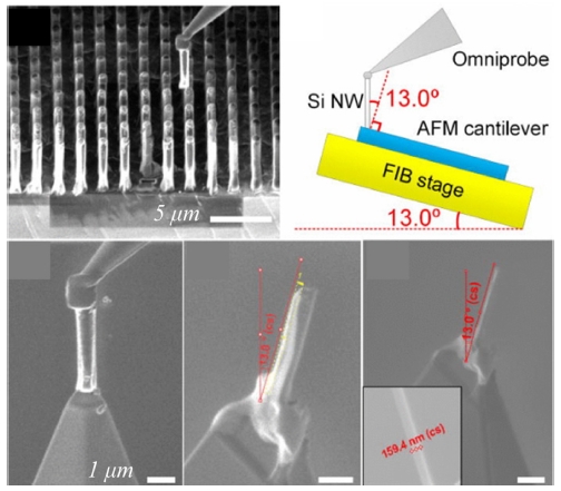
FIB 기술은 수 나노급 직경의 원자 힘 현미경(Atomic Force Microscope, AFM)용 탐침 제조에도 활용되었다. 고경도 재료인 텅스텐을 이용하여 AFM용 탐침을 제작하는데 FIB 가공 기술이 활용되었다.
66 원통형의 텅스텐 구조에 빔을 조사하여 끝 단을 직경이 5 nm이 되도록 재료 제거 공정을 수행했다.
Fig. 11과 같이 나노 와이어와 같은 고 세장비의 구조물을 FIB 장비 내부에서 탐침에 직접 붙이고 끝 단에 이온 빔을 조사하여 뾰족한 구조를 제작할 수 있다.
67 탐침에 나노 와이어를 합성하고 단일 와이어가 남도록 주변 부를 FIB로 제거하는 연구도 수행되었다.
68 이처럼 FIB를 이용한 AFM용 탐침 제조 공정들이 다양하게 제안되었다.
Fig. 11Fabrication process of nanowire AFM probe 159.4 nm by FIB; cut, attachment, transferring, and FIB milling67 (Adapted from Ref. 67 with permission)

3.2.2 광학 재료 가공
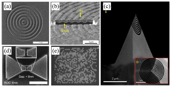
나노 광학 분야에서 FIB는 고기능, 고성능 광학 패턴의 설계과정에 필요한 프로토타이핑 도구로 활용되고 있다. 포토리소그래피 공정은 광학 패턴 설계를 최적화하는 과정에서 마스크를 수정하는 등의 추가 비용이 소요되지만, FIB 가공기술은 직접 묘사 기술이므로 추가 비용 없이 설계 변경이 가능하다. 따라서 초미세 광학 소자에 적용할 수 있는 복잡한 패턴을 설계하는 연구에서 FIB 가공기술을 활용한 사례가 많다.
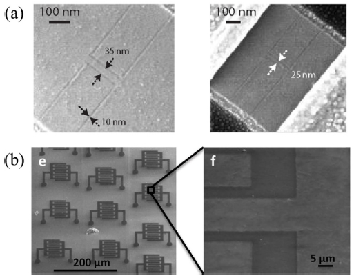
Fig. 12는 FIB 가공기술로 제작된 금속 나노 광학 구조물의 예를 보여준다. 이들 구조물은 유리 기판,
69 광섬유,
70 실리콘 AFM 탐침
71등에 코팅된 금속 박막에 나노 패턴을 제작한 결과를 나타낸다. 나노 어퍼쳐 및 그루브는 입사광을 서브 파장의 크기로 집중시키는 나노 렌즈 소자의 패턴으로 제안되었고,
72 나노 홀 어레이는 파장에 따른 나노 광 필터 소자의 패턴으로 제안되었다.
73 이들 나노 구조물은 표면 플라즈몬 공명(Surface Plasmon Resonance)현상을 기반으로 하는 초미세 광학 소자이며, 나노 패턴을 포함한 금속 박막이 광학 재료에 제작된다는 특징을 가진다. 이처럼 FIB가공 기술은 나노 광학 분야 중에서도 특히 플라즈모닉 소자 연구에서 프로토타이핑 기술로 활용되고 있으며, 주로 금속 박막에 2차원 또는 2.5차원의 복잡한 형태의 패턴을 제작하는 공정으로 활용되고 있다.
Fig. 12Nanostructures fabricated by FIB milling69-73 (Adapted from Refs. 69, 70, 71, 72, and 73 with permission)

FIB 기술은 자유형상(Freeform)의 광학 부품 제조에도 활용된다. 대표적인 부품으로는 다이아몬드 고체 침지 렌즈(Solid Immersion Lens, SIL)가 있다. SIL은 높은 개구수(Numerical Aperture, NA)를 가지는 렌즈로 반구 형태로 가공되어야 한다. 최근 단광자 방출소자로 활용되는 음으로 하전된 질소가 빈 중심(Negatively Charged Nitrogen-Vacancy Center, NV)을 가진 다이아몬드 SIL를 FIB 기술로 제작하려는 연구가 있다.
Fig. 13은 단결정 다이아몬드에 제작된 SIL의 현미경 이미지(좌)와 형광 이미지(우)를 나타낸다. 중심에 NV이 포함되어 있는 10 μm 직경의 반구형 SIL이 정밀하게 제작되었다.
74 같은 크기의 다이아몬드 SIL을 빔 전류 2.7 nA의 갈륨 이온 빔으로 가공 시, 약 60분의 가공 시간이 소요된다고 보고되었다.
75
Fig. 13Microscopic structures fabricated by FIB milling of a SIL with NV74 (Adapted from Ref. 74 with permission)

3.2.3 반도체 재료 가공
반도체 분야에서 FIB는 주로 집적 회로 수정을 위한 기술로 사용되어 왔다.
76 집적 회로의 결함을 식별하거나, 디버그 및 유효성 검사를 수행하기 위해 회로를 미세하게 절단 또는 생성하는데 LMIS 또는 GFIS FIB 가공 기술이 활용된다.
77-79 또한, 그래핀,
80MoS
2,81 ReS
282 등의 2차원 소재를 이용한 반도체 미세 소자에 대한 연구가 늘어나면서, 이들 2차원 소재기반 미세 소자 제작에 FIB 를 활용하는 연구도 수행되고 있다.
83,84
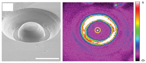
Fig. 14는 FIB로 제작된 2차원 소재기반 미세 소자의 현미경 이미지이다.
85,86 캡슐화된 그래핀 시료에 He 이온 빔을 이용하여 길이 200 nm, 너비 10-90 nm의 나노 리본 들을 제작하였고, 각각의 전기적 특성을 분석하였다.
85 그래핀의 대체 물질로 연구되고 있는 MoS
2의 두께를 얇게 하는 공정에도 FIB 가공 기술이 사용되었는데, 이온 빔 조건을 조절하면 MoS
2 시료를 원자층 두께만큼씩 제거할 수 있음을 확인하였다.
87 하지만, 여전히 이온 빔 조사에 의한 표면 손상이 2차원 소재기반 미세 소자의 특성에 미치는 영향에 대한 연구가 활발히 진행되고 있다.
88,89
Fig. 142D-material-based devices fabricated by FIB: (a) graphene nanoribbons fabricated by He ion beam and (b) graphene supercapacitors fabricated by Ga ion beam85,86 (Adapted from Refs. 85 and 86 with permission)

3.3 집속 이온 빔 정밀도 및 생산성 향상
이처럼 FIB가공 기술은 기계가공, 광학, 반도체 등의 여러 분야에서 높은 정밀도를 가진 프로토타이핑 기술로 사용되고 있다. 하지만, 여전히 가공 정밀도를 향상시키고자 하는 연구가 수행되고 있다.
우선, FIB 가공 기술의 형상 정밀도 향상을 위해 FIB 가공 형상 예측 시뮬레이션이 제안되었다.
90-93 제안된 시뮬레이션들은 이온 종류, 가속전압, 전류 등의 입사 빔의 조건과 스퍼터링율, 표면 결합 에너지, 표면 형상 등의 시료의 조건을 이용하여 가공 형상을 예측하였다. Z map 기법, 레벨 셋 기법(Level Set Method)등의 다양한 기법을 기반으로 소프트웨어를 개발하였고, 설계된 패턴을 정밀하게 가공하기 위한 이온 빔 조건을 최적화기 위해 활용되었다.
94
최근 금속 박막을 이용하여 형상 정밀도를 향상시키는 연구도 수행되었다.
95 특히, 대상 시료가 광학 및 바이오 소재와 같이 비전도성 소재일 경우 금속 박막 코팅은 필수적인 전처리 공정이기 때문에, 금속 박막을 입힌 시료의 가공 기술에 대한 연구가 수행될 필요가 있다. 이온 빔 스팟 사이즈보다 작은 너비를 가지는 채널을 가공하거나,
96 가공한 채널의 벽면을 수직하게 가공하기 위해
97 대상 시료에 금속박막을 입혀 가공한 뒤, 박막을 제거하여 정밀한 패턴을 얻는 이용하는 연구들이 수행되었다.
FIB 가공 기술의 가장 큰 단점은 가공 속도가 느려 생산성이 낮다는 것이다. 이를 극복하기 위해 다중 이온 빔을 포함하는 시스템을 개발하기 위한 연구가 수행되어 왔다.
98,99 Fig. 15는 이온 빔 3개를 동시에 조사하는 다중 빔 시스템의 예를 보여준다.
100 에프티랩은 연세대와 함께 정부 과제의 일환으로 다중빔 연마 및 밀링 장치를 개발하였다. 3개의 이온 빔을 개별적으로 구동할 수 있기 때문에, 각각의 이온 빔이 밀링 및 연마 기능을 동시에 구동할 수 있어 공정 시간을 단축시킬 수 있다는 장점을 가진다.
Fig. 15Photos of the multiple (a) ion guns and (b) ion beams100 (Adapted from Ref. 100 on the basis of open access)

4. 결론
최근 전통 초미세 부품 제조 기술의 가공 속도, 가공 소재 등의 한계를 극복하기 위한 대안으로 에너지 빔 기술에 대한 연구가 수행되어왔다. 이 논문에서는 전자 빔 및 이온 빔을 이용한 에너지 빔 가공 기술 현황에 대해 조사하였다.
전자 빔 장비는 빔 원에 따라 열 음극 전자 빔 장비와 냉 음극 전자 장비로 구분된다. 또한, 전자 빔 출력 및 파워 밀도에 따라 드릴링, 용접, 표면 처리, 적층 공정 장비로 구분된다. 저 출력의 냉 음극 전자 빔 장비 개발에 대한 연구와 플라즈마 폭발 음극 방식의 전자 빔 장비를 이용한 표면 처리 기술에 대한 연구가 있었다. 또한, 티타늄 합금, 코발트 합금 등의 다양한 종류의 메탈을 적층하여 3차원 형상의 구조물을 제작하는 전자 빔 적층 공정에 대한 연구가 수행되어 왔다. 전자 빔 가공공정은 레이저 가공공정과의 생산 단가, 제품 성능 및 생산 속도 측면에서 비교가 활발히 되고 있으며, 특히 단점으로 고가의 진공 장비가 필수적인 점을 들고 있다. 그러나 진공으로 인한 공정 후 소재의 기계적 특성 개선 등을 이유로 레이저 용접 공정에서 진공을 사용하는 사례 또한 나타나고 있다.
집속 이온 빔 장비는 빔 원에 따라 액체 금속 이온과 가스 장 이온 빔 장비로 구분된다. 또한, 이온 빔의 가속전압 및 전류에 따라 빔 크기가 결정되는데 이는 집속 이온 빔을 이용한 패터닝 기술의 가공 정밀도와 상관관계가 있다. 집속 이온 빔을 이용하여 고경도 재료, 광학 재료, 반도체 재료 등의 다양한 소재에 초 미세 구조물을 제작하는 연구가 활발히 수행되어 왔다. 또한, 집속 이온 빔 가공 형상 예측 시뮬레이션에 대한 연구를 통해 가공 정밀도를 개선하려는 노력이 있다. 하지만 여전히 이온 빔 장비는 가공 속도 및 생산성에 대해 한계를 갖고 있다. 이를 극복하기 위해, 다중 빔 장치를 이용하여 생산성을 향상시키기 위한 연구도 수행되고 있으나 여전히 연구 단계에 머물러 있다.
이처럼 전자 빔 및 이온 빔을 이용하여 기존의 전통 가공 기술이나 레이저 가공 기술의 한계를 극복하기 위한 연구가 계속 될 것이며, 결과적으로, 전자 빔 및 이온 빔 가공 기술은 초미세 고정밀 제조 기술로 첨단 신소재 부품을 제작하는 데 필수적인 기술로 자리매김 할 것으로 기대된다.
ACKNOWLEDGMENTS
본 연구는 한국 이산화탄소 포집 및 처리 연구개발 센터(Korea Carbon Capture and Sequestration Research and Development Center)의 지원과 산업통상자원부의 시스템산업 미래성장동력사업(No. 10053248, 과제명: 탄소섬유복합재(CFRP) 가공시스템 개발) 및 산업핵심기술개발 사업(No. 10063367, 과제명: 고출력 전자빔을 이용한 고세장비 미세홀 가공장비 및 공정기술 개발)의 지원으로 수행되었다.
REFERENCES
- 1.
Uriondo, A., Esperon-Miguez, M., and Perinpanayagam, S., “The Present and Future of Additive Manufacturing in the Aerospace Sector: A Review of Important Aspects,” Proceedings of the Institution of Mechanical Engineers, Part G: Journal of Aerospace Engineering, Vol. 229, No. 11, pp. 2132-2147, 2015.
10.1177/0954410014568797
- 2.
Mandil, G., Paris, H., and Suard, M., “Building New Entities from Existing Titanium Part by Electron Beam Melting: Microstructures and Mechanical Properties,” International Journal of Advanced Manufacturing Technology, Vol. 85, Nos. 5-8, pp. 1835-1846, 2016.
10.1007/s00170-015-8049-3
- 3.
Packianather, M., Le, C., Pham, D. T., and Le, H. Q., “Advanced Micro and Nano Manufacturing Technologies Used in Medical Domain,” Proc. of International Conference on the Development of Biomedical Engineering in Vietnam, pp. 637-642, 2017.
10.1007/978-981-10-4361-1_109
- 4.
Mishra, S. and Yadava, V., “Laser Beam Micromachining (LBMM)–A Review,” Optics and Lasers in Engineering, Vol. 73, pp. 89-122, 2015.
10.1016/j.optlaseng.2015.03.017
- 5.
Kim, J., Lee, W. J., and Park, H. W., “The State of the Art in the Electron Beam Manufacturing Processes,” Int. J. Precis. Eng. Manuf., Vol. 17, No. 11, pp. 1575-1585, 2016.
10.1007/s12541-016-0184-8
- 6.
Bruchhaus, L., Mazarov, P., Bischoff, L., Gierak, J., Wieck, A., et al., “Comparison of Technologies for Nano Device Prototyping with a Special Focus on Ion Beams: A Review,” Applied Physics Reviews, Vol. 4, No. 1, Paper No. 011302, 2017.
10.1063/1.4972262
- 7.
Körner, C., “Additive Manufacturing of Metallic Components by Selective Electron Beam Melting-A Review,” International Materials Reviews, Vol. 61, No. 5, pp. 361-377, 2016.
10.1080/09506608.2016.1176289
- 8.
Gao, S. and Huang, H., “Recent Advances in Micro-and Nano-Machining Technologies,” Frontiers of Mechanical Engineering, Vol. 12, No. 1, pp. 18-32, 2017.
10.1007/s11465-017-0410-9
- 9.
Futamoto, M., Nakazawa, M., Usami, K., Hosoki, S., and Kawabe, U., “Thermionic Emission Properties of a Single Crystal LaB6 Cathode,” Journal of Applied Physics, Vol. 51, No. 7, pp. 3869-3876, 1980.
10.1063/1.328132
- 10.
Iiyoshi, R. and Maruse, S., “Tungsten-Point-Cathode Electron Gun Using Electron Bombardment for Cathode Tip Heating: Cathode Life and Operating Characteristics at Cathode Temperatures Above 2,800 k,” Microscopy, Vol. 45, No. 2, pp. 128-134, 1996.
10.1093/oxfordjournals.jmicro.a023421
- 11.
Melnyk, V., Melnyk, I., Tugai, B., and Kovalchuk, D., “Recent Progress in Development of Gas-Discharge Electron Beam Guns Providing Extension of their Technological Capabilities,” Proc. of 11th International Conference on Electron Beam Technologies, 2014.
- 12.
Rodriguez, S. D. P., “Investigation and Optimisation of a Plasma Cathode Electron Beam Gun for Material Processing Applications,” Ph.D. Thesis, Brunel University London, 2016.
- 13.
Kang, E. G., “High Voltage Plasma Diode Electron Beam Accelerator and Application to Tool Steel Heat Treatment,” Ph.D. Thesis, Yonsei University, 2017.
- 14.
Walton, S., Boris, D., Hernández, S., Lock, E., Petrova, T. B., et al., “Electron Beam Generated Plasmas for Ultra Low Te Processing,” ECS Journal of Solid State Science and Technology, Vol. 4, No. 6, pp. 5033-5040, 2015.
10.1149/2.0071506jss
- 15.
Okada, A., Yonehara, H., and Okamoto, Y., “Fundamental Study on Micro-Deburring by Large-Area EB Irradiation,” Procedia CIRP, Vol. 5, pp. 19-24, 2013.
10.1016/j.procir.2013.01.004
- 16.
Bataev, I., Golkovskii, M., Bataev, A., Losinskaya, A., Dostovalov, R., et al., “Surface Hardening of Steels with Carbon by Non-Vacuum Electron-Beam Processing,” Surface and Coatings Technology, Vol. 242, pp. 164-169, 2014.
10.1016/j.surfcoat.2014.01.038
- 17.
Kim, J., Kim, J.-S., Kang, E.-G., and Park, H. W., “Surface Modification of the Metal Plates Using Continuous Electron Beam Process (CEBP),” Applied Surface Science, Vol. 311, pp. 201-207, 2014.
10.1016/j.apsusc.2014.05.041
- 18.
Okada, A., Okamoto, Y., Uno, Y., and Uemura, K., “Improvement of Surface Characteristics for Long Life of Metal Molds by Large-Area EB Irradiation,” Journal of Materials Processing Technology, Vol. 214, No. 8, pp. 1740-1748, 2014.
10.1016/j.jmatprotec.2014.02.028
- 19.
Cheng, B. and Chou, K., “Geometric Consideration of Support Structures in Part Overhang Fabrications by Electron Beam Additive Manufacturing,” Computer-Aided Design, Vol. 69, pp. 102-111, 2015.
10.1016/j.cad.2015.06.007
- 20.
Ahn, Y.-K., Kim, H.-G., Park, H.-K., Kim, G.-H., Jung, K.-H., et al., “Mechanical and Microstructural Characteristics of Commercial Purity Titanium Implants Fabricated by Electron-Beam Additive Manufacturing,” Materials Letters, Vol. 187, pp. 64-67, 2017.
10.1016/j.matlet.2016.10.064
- 21.
Park, H. K., Ahn, Y. K., Lee, B. S., Jung, K. H., Lee, C. W., et al., “Refining Effect of Electron Beam Melting on Additive Manufacturing of Pure Titanium Products,” Materials Letters, Vol. 187, pp. 98-100, 2017.
10.1016/j.matlet.2016.10.065
- 22.
Koleva, E., Mladenov, G., and Vutova, K., “Calculation of Weld Parameters and Thermal Efficiency in Electron Beam Welding,” Vacuum, Vol. 53, Nos. 1-2, pp. 67-70, 1999.
10.1016/S0042-207X(98)00393-5
- 23.
Koleva, E., “Electron Beam Weld Parameters and Thermal Efficiency Improvement,” Vacuum, Vol. 77, No. 4, pp. 413-421, 2005.
10.1016/j.vacuum.2004.09.002
- 24.
Ho, J. E. and Young, H. T., “The Analysis on Penetrating Efficiency in High-Energy Beam Drilling,” Key Engineering Materials, pp. 308-314, 2008.
- 25.
- 26.
Kang, E. G., “High Speed Ecological Finishing Process Technology Development of High Density Electron Beam for Precision Machine Parts Processing,” Proc. of the Korean Society of Manufacturing Technology Engineers Spring Conference, p. 79, 2016.
- 27.
Kang, E. G., Choi, H., Min, B.-K., and Lee, S. J., “Austenite Phase Transformation of SKD11 by Surface Heat Treatment with a Focused Electron Beam,” Surface and Coatings Technology, Vol. 321, pp. 247-256, 2017.
10.1016/j.surfcoat.2017.03.042
- 28.
Gao, B., Hao, Y., Tu, G., and Wu, W., “Study on Nanostructures Induced by High-Current Pulsed Electron Beam,” Journal of Nanomaterials, p. 5, 2012.
10.1155/2012/480482
- 29.
Zhang, C., Gao, Q., Lv, P., Cai, J., Peng, C.-T., et al., “Surface Modification of Cu-W Powder Metallurgical Alloy Induced by High-Current Pulsed Electron Beam,” Powder Technology, Vol. 325, pp. 340-346, 2018.
10.1016/j.powtec.2017.11.037
- 30.
Zhang, C., Lv, P., Cai, J., Peng, C.-T., Jin, Y., et al., “The Microstructure and Properties of Tungsten Alloying Layer on Copper by High-Current Pulse Electron Beam,” Applied Surface Science, Vol. 422, pp. 582-590, 2017.
10.1016/j.apsusc.2017.06.049
- 31.
Tang, G., Luo, D., Tang, S., Mu, Q., Wang, L., et al., “The Microstructure and Properties of Cr Alloying Layer After Surface Alloying Treatment Induced by High Current Pulsed Electron Beam,” Journal of Alloys and Compounds, Vol. 714, pp. 96-103, 2017.
10.1016/j.jallcom.2017.04.014
- 32.
Hao, S., Wang, H., and Zhao, L., “Surface Modification of 40CrNiMo7 Steel with High Current Pulsed Electron Beam Treatment,” Nuclear Instruments and Methods in Physics Research Section B: Beam Interactions with Materials and Atoms, Vol. 368, pp. 81-85, 2016.
10.1016/j.nimb.2015.11.039
- 33.
Zhang, K., Ma, J., Zou, J., and Liu, Y., “Surface Microstructure and Property Modifications in a Duplex Stainless Steel Induced by High Current Pulsed Electron Beam Treatments,” Journal of Alloys and Compounds, Vol. 707, pp. 178-183, 2017.
10.1016/j.jallcom.2017.01.003
- 34.
Xia, H., Zhang, C., Lv, P., Cai, J., Jin, Y., et al., “Surface Alloying of Aluminum with Molybdenum by High-Current Pulsed Electron Beam,” Nuclear Instruments and Methods in Physics Research Section B: Beam Interactions with Materials and Atoms, Vol. 416, pp. 9-15, 2018.
10.1016/j.nimb.2017.11.028
- 35.
- 36.
Lewandowski, J. J. and Seifi, M., “Metal Additive Manufacturing: A Review of Mechanical Properties,” Annual Review of Materials Research, Vol. 46, pp. 151-186, 2016.
10.1146/annurev-matsci-070115-032024
- 37.
Edwards, P., O'Conner, A., and Ramulu, M., “Electron Beam Additive Manufacturing of Titanium Components: Properties and Performance,” Journal of Manufacturing Science and Engineering, Vol. 135, No. 6, Paper No. 061016, 2013.
10.1115/1.4025773
- 38.
Murr, L. E., Gaytan, S. M., Ramirez, D. A., Martinez, E., Hernandez, J., et al., “Metal Fabrication by Additive Manufacturing Using Laser and Electron Beam Melting Technologies,” Journal of Materials Science & Technology, Vol. 28, No. 1, pp. 1-14, 2012.
10.1016/S1005-0302(12)60016-4
- 39.
Zhong, Y., Rännar, L.-E., Liu, L., Koptyug, A., Wikman, S., et al., “Additive Manufacturing of 316L Stainless Steel by Electron Beam Melting for Nuclear Fusion Applications,” Journal of Nuclear Materials, Vol. 486, pp. 234-245, 2017.
10.1016/j.jnucmat.2016.12.042
- 40.
Lee, H.-J., Song, J.-G., Kim, J.-S., and Ahn, D.-G., “Preliminary Study on Pre-Heating Process of Stellite21 Powder Using Electron Beam,” J. Korean Soc. Precis. Eng., Vol. 33, No. 5, pp. 419-425, 2016.
10.7736/KSPE.2016.33.5.419
- 41.
Lee, H.-J., Ahn, D.-G., Song, J.-G., Kim, J.-S., and Kang, E. G., “Fabrication of Beads Using a Plasma Electron Beam and Stellite21 Powders for Additive Manufacturing,” Int. J. Precis. Eng. Manuf.-Green Tech., Vol. 4, No. 4, pp. 453-456, 2017.
10.1007/s40684-017-0050-x
- 42.
Cordero, Z. C., Meyer, H. M., Nandwana, P., and Dehoff, R. R., “Powder Bed Charging during Electron-Beam Additive Manufacturing,” Acta Materialia, Vol. 124, pp. 437-445, 2017.
10.1016/j.actamat.2016.11.012
- 43.
Zhao, S., Li, S., Hou, W., Hao, Y., Yang, R., et al., “The Influence of Cell Morphology on the Compressive Fatigue Behavior of Ti-6Al-4V Meshes Fabricated by Electron Beam Melting,” Journal of the Mechanical Behavior of Biomedical Materials, Vol. 59, pp. 251-264, 2016.
10.1016/j.jmbbm.2016.01.034
- 44.
Cheng, B., Price, S., Lydon, J., Cooper, K., and Chou, K., “On Process Temperature in Powder-Bed Electron Beam Additive Manufacturing: Model Development and Validation,” Journal of Manufacturing Science and Engineering, Vol. 136, No. 6, Paper No. 061018, 2014.
10.1115/1.4028484
- 45.
Raplee, J., Plotkowski, A., Kirka, M. M., Dinwiddie, R., Okello, A., et al., “Thermographic Microstructure Monitoring in Electron Beam Additive Manufacturing,” Scientific Reports, Vol. 7, Article No. 43554, 2017.
10.1038/srep43554
- 46.
Singh, R., Akhgar, A., Sui, P., Lange, K., and Djilali, N., “Dual-Beam FIB/SEM Characterization, Statistical Reconstruction, and Pore Scale Modeling of a PEMFC Catalyst Layer,” Journal of The Electrochemical Society, Vol. 161, No. 4, pp. 415-424, 2014.
10.1149/2.036404jes
- 47.
Kurpaska, L., Jozwik, I., and Jagielski, J., “Study of Sub-Oxide Phases at the Metal-Oxide Interface in Oxidized Pure Zirconium and Zr-1.0% Nb Alloy by Using SEM/FIB/EBSD and EDS Techniques,” Journal of Nuclear Materials, Vol. 476, pp. 56-62, 2016.
10.1016/j.jnucmat.2016.04.038
- 48.
Gelb, J., Finegan, D. P., Brett, D. J., and Shearing, P. R., “Multi-Scale 3D Investigations of a Commercial 18650 Li-Ion Battery with Correlative Electron-and X-Ray Microscopy,” Journal of Power Sources, Vol. 357, pp. 77-86, 2017.
10.1016/j.jpowsour.2017.04.102
- 49.
Shen, K., Wucher, A., and Winograd, N., “Molecular Depth Profiling with Argon Gas Cluster Ion Beams,” Journal of Physical Chemistry C, Vol. 119, No. 27, pp. 15316-15324, 2015.
10.1021/acs.jpcc.5b03482
- 50.
Nastasi, M., Mayer, J., and Hirvonen, J. K., “Ion-Solid Interactions: Fundamentals and Applications,” Cambridge University Press, 1996.
10.1017/CBO9780511565007
- 51.
Volkert, C. A. and Minor, A. M., “Focused Ion Beam Microscopy and Micromachining,” MRS Bulletin, Vol. 32, No. 5, pp. 389-399, 2007.
10.1557/mrs2007.62
- 52.
Livengood, R., Tan, S., Greenzweig, Y., Notte, J., and McVey, S., “Subsurface Damage from Helium Ions as a Function of Dose, Beam Energy, and Dose Rate,” Journal of Vacuum Science & Technology B: Microelectronics and Nanometer Structures Processing, Measurement, and Phenomena, Vol. 27, No. 6, pp. 3244-3249, 2009.
10.1116/1.3237101
- 53.
Tan, S., Livengood, R., Shima, D., Notte, J., and McVey, S., “Gas Field Ion Source and Liquid Metal Ion Source Charged Particle Material Interaction Study for Semiconductor Nanomachining Applications,” Journal of Vacuum Science & Technology B, Nanotechnology and Microelectronics: Materials, Processing, Measurement, and Phenomena, Vol. 28, No. 6, pp. C6F15-C16F21, 2010.
10.1116/1.3511509
- 54.
Boden, S., Moktadir, Z., Bagnall, D., Mizuta, H., and Rutt, H., “Focused Helium Ion Beam Milling and Deposition,” Microelectronic Engineering, Vol. 88, No. 8, pp. 2452-2455, 2011.
10.1016/j.mee.2010.11.041
- 55.
Bassim, N., Scott, K., and Giannuzzi, L. A., “Recent Advances in Focused Ion Beam Technology and Applications,” MRS Bulletin, Vol. 39, No. 4, pp. 317-325, 2014.
10.1557/mrs.2014.52
- 56.
Li, H., Wani, I. H., Hayat, A., Jafri, S. H. M., and Leifer, K., “Fabrication of Reproducible Sub-5 nm Nanogaps by a Focused Ion Beam and Observation of Fowler-Nordheim Tunneling,” Applied Physics Letters, Vol. 107, No. 10, Paper No. 103108, 2015.
10.1063/1.4930821
- 57.
Adams, D. P., Vasile, M. J., Benavides, G., and Campbell, A. N., “Micromilling of Metal Alloys with Focused Ion Beam-Fabricated Tools,” Precision Engineering, Vol. 25, No. 2, pp. 107-113, 2001.
10.1016/S0141-6359(00)00064-7
- 58.
Picard, Y. N., Adams, D., Vasile, M., and Ritchey, M., “Focused Ion Beam-Shaped Microtools for Ultra-Precision Machining of Cylindrical Components,” Precision Engineering, Vol. 27, No. 1, pp. 59-69, 2003.
10.1016/S0141-6359(02)00188-5
- 59.
Sun, J., Luo, X., Chang, W., Ritchie, J., Chien, J., et al., “Fabrication of Periodic Nanostructures by Single-Point Diamond Turning with Focused Ion Beam Built Tool Tips,” Journal of Micromechanics and Microengineering, Vol. 22, No. 11, Paper No. 115014, 2012.
10.1088/0960-1317/22/11/115014
- 60.
Choi, W. K. and Baek, S. Y., “Study on Platinum Coating Depth in Focused Ion Beam Diamond Cutting Tool Milling and Methods for Removing Platinum Layer,” Materials, Vol. 8, No. 9, pp. 6498-6507, 2015.
10.3390/ma8095317
- 61.
Luo, X., Tong, Z., and Liang, Y., “Investigation of the Shape Transferability of Nanoscale Multi-Tip Diamond Tools in the Diamond Turning of Nanostructures,” Applied Surface Science, Vol. 321, pp. 495-502, 2014.
10.1016/j.apsusc.2014.10.052
- 62.
McKenzie, W., Quadir, M. Z., Gass, M., and Munroe, P., “Focused Ion Beam Implantation of Diamond,” Diamond and Related Materials, Vol. 20, No. 8, pp. 1125-1128, 2011.
10.1016/j.diamond.2011.06.022
- 63.
Tong, Z. and Luo, X., “Investigation of Focused Ion Beam Induced Damage in Single Crystal Diamond Tools,” Applied Surface Science, Vol. 347, pp. 727-735, 2015.
10.1016/j.apsusc.2015.04.120
- 64.
Kawasegi, N., Ozaki, K., Morita, N., Nishimura, K., and Sasaoka, H., “Single-Crystal Diamond Tools Formed Using a Focused Ion Beam: Tool Life Enhancement via Heat Treatment,” Diamond and Related Materials, Vol. 49, pp. 14-18, 2014.
10.1016/j.diamond.2014.07.013
- 65.
Martin, A. A., Randolph, S., Botman, A., Toth, M., and Aharonovich, I., “Maskless Milling of Diamond by a Focused Oxygen Ion Beam,” Scientific Reports, Vol. 5, Article No. 8958, 2015.
10.1038/srep08958
- 66.
Ageev, O., Kolomiytsev, A. S., Bykov, A., Smirnov, V., and Kots, I., “Fabrication of Advanced Probes for Atomic Force Microscopy Using Focused Ion Beam,” Microelectronics Reliability, Vol. 55, Nos. 9-10, pp. 2131-2134, 2015.
10.1016/j.microrel.2015.06.079
- 67.
Tan, S. C., Zhao, H., and Thompson, C. V., “Fabrication of High Aspect Ratio AFM Probes with Different Materials Inspired by Tem “Lift-Out” Method,” Journal of Vacuum Science & Technology B, Nanotechnology and Microelectronics: Materials, Processing, Measurement, and Phenomena, Vol. 34, No. 5, Paper No. 051805, 2016.
10.1116/1.4961595
- 68.
Knittel, P., Hibst, N., Mizaikoff, B., Strehle, S., and Kranz, C., “Focused Ion Beam-Assisted Fabrication of Soft High-Aspect Ratio Silicon Nanowire Atomic Force Microscopy Probes,” Ultramicroscopy, Vol. 179, pp. 24-32, 2017.
10.1016/j.ultramic.2017.03.031
- 69.
Pournoury, M., Joe, H.-E., Park, J. H., Nazari, T., Sung, Y. M., et al., “Polarization-Dependent Transmission through a Bull's Eye with an Elliptical Aperture,” Optics Communications, Vol. 316, pp. 1-4, 2014.
10.1016/j.optcom.2013.10.081
- 70.
Arabi, H. E., Joe, H.-E., Nazari, T., Min, B.-K., and Oh, K., “A High Throughput Supra-Wavelength Plasmonic Bull’S Eye Photon Sorter Spatially and Spectrally Multiplexed on Silica Optical Fiber Facet,” Optics Express, Vol. 21, No. 23, pp. 28083-28094, 2013.
10.1364/OE.21.028083
- 71.
Zhao, Y., Saleh, A. A., van de Haar, M. A., Baum, B., Briggs, J. A., et al., “Nanoscopic Control and Quantification of Enantioselective Optical Forces,” Nature Nanotechnology, Vol. 12, No. 11, Article No. 1055, 2017.
10.1038/nnano.2017.180
- 72.
Kollmann, H., Piao, X., Esmann, M., Becker, S. F., Hou, D., et al., “Toward Plasmonics with Nanometer Precision: Nonlinear Optics of Helium-Ion Milled Gold Nanoantennas,” Nano Letters, Vol. 14, No. 8, pp. 4778-4784, 2014.
10.1021/nl5019589
- 73.
Yokogawa, S., Burgos, S. P., and Atwater, H. A., “Plasmonic Color Filters for CMOS Image Sensor Applications,” Nano Letters, Vol. 12, No. 8, pp. 4349-4354, 2012.
10.1021/nl302110z
- 74.
Jiang, Q., Liu, D., Liu, G., Chang, Y., Li, W., et al., “Focused-Ion-Beam Overlay-Patterning of Three-Dimensional Diamond Structures for Advanced Single-Photon Properties,” Journal of Applied Physics, Vol. 116, No. 4, Paper No. 044308, 2014.
10.1063/1.4891022
- 75.
Jamali, M., Gerhardt, I., Rezai, M., Frenner, K., Fedder, H., et al., “Microscopic Diamond Solid-Immersion-Lenses Fabricated around Single Defect Centers by Focused Ion Beam Milling,” Review of Scientific Instruments, Vol. 85, No. 12, Paper No. 123703, 2014.
10.1063/1.4902818
- 76.
Livengood, R., Tan, S., Hack, P., Kane, M., and Greenzweig, Y., “Focused Ion Beam Circuit Edit-A Look into the Past, Present, and Future,” Microscopy and Microanalysis, Vol. 17, No. S2, pp. 672-673, 2011.
10.1017/S1431927611004235
- 77.
Wu, H., Ferranti, D., and Stern, L., “Precise Nanofabrication with Multiple Ion Beams for Advanced Circuit Edit,” Microelectronics Reliability, Vol. 54, Nos. 9-10, pp. 1779-1784, 2014.
10.1016/j.microrel.2014.08.003
- 78.
Wu, H., Stern, L., Xia, D., Ferranti, D., Thompson, B., et al., “Focused Helium Ion Beam Deposited Low Resistivity Cobalt Metal Lines with 10 nm Resolution: Implications for Advanced Circuit Editing,” Journal of Materials Science: Materials in Electronics, Vol. 25, No. 2, pp. 587-595, 2014.
10.1007/s10854-013-1522-6
- 79.
Xia, D., Wu, H., Geotze, B., Ferranti, D., Stern, L., et al., “Circuit Editing and Failure Analysis Applications Using a Three-Ion-Beam (Ga, He and Ne) System and Gas Injection System (GIS),” Microscopy and Microanalysis, Vol. 21, Article No. 1165, 2015.
10.1017/S1431927615006613
- 80.
Zhu, Z., Murtaza, I., Meng, H., and Huang, W., “Thin Film Transistors Based on Two Dimensional Graphene and Graphene/Semiconductor Heterojunctions,” RSC Advances, Vol. 7, No. 28, pp. 17387-17397, 2017.
10.1039/C6RA27674A
- 81.
Yoon, H. S., Joe, H.-E., Kim, S. J., Lee, H. S., et al., “Layer Dependence and Gas Molecule Absorption Property in MoS2 Schottky Diode with Asymmetric Metal Contacts,” Scientific Reports, Vol. 5, Paper No. 10440, 2015.
10.1038/srep10440
- 82.
Park, J. Y., Joe, H.-E., Yoon, H. S., Yoo, S., Kim, T., et al., “Contact Effect of ReS2/Metal Interface,” ACS Applied Materials & Interfaces, Vol. 9, No. 31, pp. 26325-26332, 2017.
10.1021/acsami.7b06432
- 83.
Abbas, A. N., Liu, G., Liu, B., Zhang, L., Liu, H., et al., “Patterning, Characterization, and Chemical Sensing Applications of Graphene Nanoribbon Arrays Down to 5 nm Using Helium Ion Beam Lithography,” ACS Nano, Vol. 8, No. 2, pp. 1538-1546, 2014.
10.1021/nn405759v
- 84.
Kotakoski, J., Brand, C., Lilach, Y., Cheshnovsky, O., Mangler, C., et al., “Toward Two-Dimensional All-Carbon Heterostructures via Ion Beam Patterning of Single-Layer Graphene,” Nano Letters, Vol. 15, No. 9, pp. 5944-5949, 2015.
10.1021/acs.nanolett.5b02063
- 85.
Nanda, G., Hlawacek, G., Goswami, S., Watanabe, K., Taniguchi, T., et al., “Electronic Transport in Helium-Ion-Beam Etched Encapsulated Graphene Nanoribbons,” Carbon, Vol. 119, pp. 419-425, 2017.
10.1016/j.carbon.2017.04.062
- 86.
Lobo, D. E., Banerjee, P. C., Easton, C. D., and Majumder, M., “Miniaturized Supercapacitors: Focused Ion Beam Reduced Graphene Oxide Supercapacitors with Enhanced Performance Metrics,” Advanced Energy Materials, Vol. 5, No. 19, 2015.
10.1002/aenm.201500665
- 87.
Wang, D., Wang, Y., Chen, X., Zhu, Y., Zhan, K., et al., “Layer-by-Layer Thinning of Two-Dimensional MoS2 Films by Using a Focused Ion Beam,” Nanoscale, Vol. 8, No. 7, pp. 4107-4112, 2016.
10.1039/C5NR05768J
- 88.
Amjadipour, M., MacLeod, J., Lipton-Duffin, J., Iacopi, F., and Motta, N., “Epitaxial Graphene Growth on FIB Patterned 3C-SiC Nanostructures on Si (111): Reducing Milling Damage,” Nanotechnology, Vol. 28, No. 34, Paper No. 345602, 2017.
10.1088/1361-6528/aa752e
- 89.
Gawlik, G., Ciepielewski, P., Jagielski, J., and Baranowski, J., “Modification of Graphene by Ion Beam,” Nuclear Instruments and Methods in Physics Research Section B: Beam Interactions with Materials and Atoms, Vol. 406, pp. 683-688, 2017.
10.1016/j.nimb.2017.04.054
- 90.
Han, J., Lee, H., Min, B.-K., and Lee, S. J., “Prediction of Nanopattern Topography Using Two-Dimensional Focused Ion Beam Milling with Beam Irradiation Intervals,” Microelectronic Engineering, Vol. 87, No. 1, pp. 1-9, 2010.
10.1016/j.mee.2009.05.010
- 91.
Kim, H.-B., Hobler, G., Steiger, A., Lugstein, A., and Bertagnolli, E., “Full Three-Dimensional Simulation of Focused Ion Beam Micro/Nanofabrication,” Nanotechnology, Vol. 18, No. 24, Paper No. 245303, 2007.
10.1088/0957-4484/18/24/245303
- 92.
Shumilov, A. and Amirov, I., “Morphology Simulation of the Surface Subjected to Low-Energy Ion Sputtering,” Technical Physics, Vol. 60, No. 7, pp. 1056-1062, 2015.
10.1134/S1063784215070245
- 93.
Borgardt, N. I. and Rumyantsev, A. V., “Prediction of Surface Topography due to Finite Pixel Spacing in FIB Milling of Rectangular Boxes and Trenches,” Journal of Vacuum Science & Technology B, Nanotechnology and Microelectronics: Materials, Processing, Measurement, and Phenomena, Vol. 34, No. 6, Paper No. 061803, 2016.
10.1116/1.4967249
- 94.
De Felicis, D., Mughal, M. Z., and Bemporad, E., “A Method to Improve the Quality of 2.5 Dimensional Micro-and Nano-Structures Produced by Focused Ion Beam Machining,” Micron, Vol. 101, pp. 8-15, 2017.
10.1016/j.micron.2017.05.005
- 95.
Kannegulla, A. and Cheng, L.-J., “Metal Assisted Focused-Ion Beam Nanopatterning,” Nanotechnology, Vol. 27, No. 36, pp. 36LT01, 2016.
10.1088/0957-4484/27/36/36LT01
- 96.
Menard, L. D. and Ramsey, J. M., “Fabrication of Sub-5 nm Nanochannels in Insulating Substrates Using Focused Ion Beam Milling,” Nano Letters, Vol. 11, No. 2, pp. 512-517, 2010.
10.1021/nl103369g
- 97.
Joe, H.-E., Park, J.-H., Kim, S. H., Kim, G., Jun, M. B., et al., “Effects of Coating Material on the Fabrication Accuracy of Focused Ion Beam Machining of Insulators,” Japanese Journal of Applied Physics, Vol. 54, No. 9, Paper No. 096602, 2015.
10.7567/JJAP.54.096602
- 98.
Choi, Y., Kim, T.-G., Han, J., Min, B.-K., Kim, Y.-J., et al., “Design and Fabrication of Multi-Aperture Plate for Multi-Ion Beam Patterning System,” Japanese Journal of Applied Physics, Vol. 49, No. 6S, Paper No. 06GE06, 2010.
10.1143/JJAP.49.06GE06
- 99.
Chkhalo, N., Kaskov, I., Malyshev, I., Mikhaylenko, M., Pestov, A., et al., “High-Performance Facility and Techniques for High-Precision Machining of Optical Components by Ion Beams,” Precision Engineering, Vol. 48, pp. 338-346, 2017.
10.1016/j.precisioneng.2017.01.004
- 100.