ABSTRACT
The purpose of this review paper is to highlight recent efforts and achievements to realize high productivity of micro/nano structure fabrication processes and feasible applications. Due to development in micro/nano fabrication processes, demands on micro/nano related applications are increasing rapidly in various fields. To meet requirements, fabrication process must have high production yield and be automated. Also, fabricated micro/nano structures are expressed on large area substrate. So, it is timely and appropriate to move forward to a new epoch by researching more robust and high throughput fabrication methods, large area fabrication techniques, and new applications. In this review paper, we present a series of recent achievements to overcome some of the limitations in productivity and product size of current fabrication processes, such as photolithography and imprinting lithography. For potential applications, transparent metal electrode, large size optical film, bus wire for narrow bezel, and water collecting surface, are briefly described to expand the application field from the well-known.
-
KEYWORDS: Imprint lithography, Coating process, Dispense, Doctor blade, Roll to roll process
-
KEYWORDS: 임프린트 리소그래피, 코팅 공정, 디스펜서, 닥터블레이드, 롤투롤 공정
1. 서론
1995년에 개발되어 지난 20년간 많은 연구진에 의해 발전 되어온 나노임프린트리소그래피(이하 NIL) 관련 연구는 학교나 연구소의 기초 연구를 넘어 실제 산업으로의 응용이 시작되면서 기존의 포토리소그래피와 함께 마이크로/나노 구조를 생산 하는 대표 기술로 자리매김하였다.
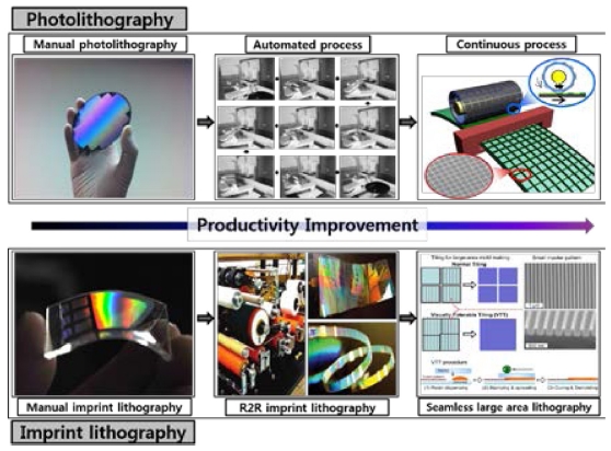
1-3 NIL은 현재 산업계에서 지배적으로 이용되고 있는 포토리소그래피(Photo Lithography)에 비해 더 작은 크기의 구조를 제작 할 수 있고, 공정이 간단하며, 비용이 저렴하다는 점에서 상대적인 장점을 가진다. 이러한 NIL 공정의 대량 생산을 위해, NIL 기술과 Roll to Roll (R2R) 방식을 접목시켜 공정을 연속적으로 처리하는 기술에 대한 연구가 많은 연구진에 의해 진행되었으며, 그 응용 대상에 따라 차이가 있지만 NIL 공정의 연속 생산 가능성에 대한 연구가 패터닝 부분을 중심으로 이미 상용화 단계에 다다랐다.
4-6 롤투롤 기반의 NIL이 개발되어 생산성에 있어서는 별다른 이슈가 발생하지 않았지만 마스터몰드를 직접적으로 접촉하여 복제하는 NIL 공정의 특성상 패턴 면적을 대면적화 하는데 한계가 있다는 문제점이 제기 되었고 이를 해결하기 위한 다양한 연구들이 발표되었다. Nanochannel Guided Lithography, Danamic Nano-Inscribing, Localized Dynamic Weinkling, Vibration Indentation-Driven Patterning 등 기존의 1 대 1 복제 공정을 탈피한 물리적 접촉기반의 연속 패터닝 기술이 그 예이다.
7-10 이들 공정은 매우 우수한 연속성과 생산성을 가지고 마스터몰드의 크기와 상관없이 넓은 면적의 마이크로/나노 패턴을 제작할 수 있다. 하지만 높은 종횡비의 구조를 제작하거나 정확히 디자인된 구조를 생산하기에는 어려움이 있다. 이런 문제를 해결하기 위하여 작은 면적의 마스터 몰드 패턴을 대면적화 시킬 수 있는 시각적관용성을 갖는 타일링 기술(Visually Tolerable Tiling, VTT)이 개발되었다.
11 이 기술은 이웃한 패턴영역 사이의 경계선을 최소화 시켜 시각적으로 관찰이 안되도록 하는 패터닝 기법으로 작은 마스터 몰드를 활용하여 대면적의 복제 몰드를 제작할 때 유용하게 활용될 수 있다. 이러한 기술을 바탕으로 하여 NIL은 상용화를 위한 생산성 향상을 도모하고 있다.
Fig. 1 A schematic diagram of the technology development process for improving the productivity of photolithography and NIL3,6,11,12 (reproduced from ref. 3, 6, 11, 12 with permission)

NIL이 개발된 이래 줄곧 비교대상이 되어오던 포토리소그래피 역시 진화를 거듭하고 있다. 반도체, 디스플레이 생산 공정에서 가장 핵심적인 부분을 담당하고 있는 포토리소그래피는 오랜 역사에 걸맞게 높은 기술 완성도를 바탕으로 미세구조 제작 공정에서 대표 기술로 자리매김하고 있고 NIL과 마찬가지로 기술의 단점을 보완하기 위하여 생산성 향상, 공정 수율 향상 등의 기술 개발이 수행되고 있다. 포토리소그래피는 공정특성상 기판 단위로 노광이 진행되는데 이러한 공정은 자동화는 가능하지만 연속적으로 이루어지기 어려워 생산성의 향상에 한계가 존재한다. 또한 자동화에 많은 비용이 들기 때문에 공정의 응용처 확산에 어려움이있다. 이를 해결하기 위해 최근 롤타입의 포토마스크를 활용한 연속 포토리소그래피 공정이 개발되었다. 이 기술은 기존의 포토리소그래피와 공정기본 원리는 같지만 평면형태의 포토마스크 대신 실린더형태의 포토마스크를 활용하여 연속공정이 가능한 롤타입의 노광 장치를 실현하였다.
3,13
NIL과 포토리소그래피 이외에도 전자인쇄, 3D 프린팅 등의 미세구조 제작 기술이 특정 응용분야에서 상용화를 위해 생산성 향상을 도모하고 있지만
14-18 이 논문에서는 Quasi-3D 구조를 제작할 수 있는 NIL과 포토리소 그래피에 대해서만 다루기로 한다.
2. 나노임프린트 리소그래피
2.1 롤투롤 나노임프린트 리소그래피
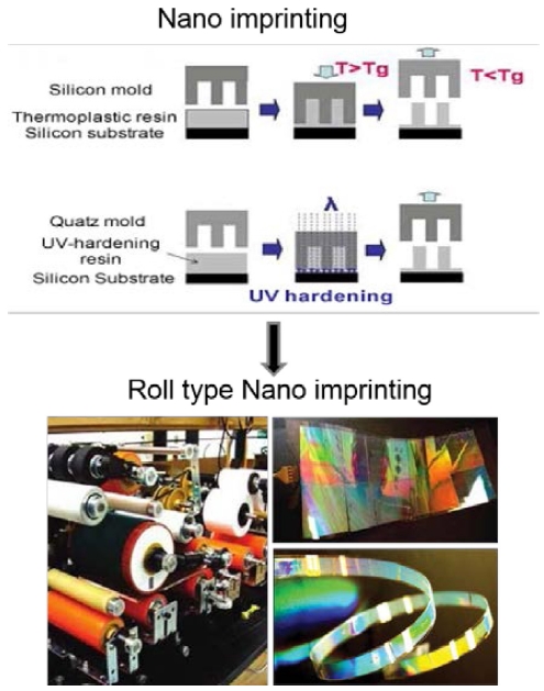
나노임프린트(NIL)는 100 nm 이하의 크기를 갖는 미세 구조를 제작할 수 있는 기술로 1995년 Stephen Chou 교수가 개발하였다.
1 그 당시 미세구조 제작 분야에서는 기존의 포토리소그래피가 갖는 광회절 한계(~100 nm)를 극복할 수 있는 기술에 대한 요구가 있었는데 이를 위해 광원 개발과 장비 개선을 통해 새로운 공정이 소개되었다. 전통적인 광학리소그래피 기술에서 개선된 공정은 대표적으로 E-Beam 리소그래피, Ion-Beam 리소그래피, EUV 리소그래피 등으로 일반적인 광회절 한계를 넘어서는 수준의 해상도를 표현할 수 있었다. 하지만 공정을 수행하기 위한 초기 비용이 매우 높은 단점이 있어 새로운 형태의 복제기반 패터닝 기술인 NIL이 선보이게 되었다. 초기 NIL 기술은 열성형 방식으로 임의의 기판위에 열가소성 수지를 코팅하고 그 위에 나노 구조가 형성된 마스터 몰드를 접촉시킨 후 가열/냉각하여 마스터의 역상을 복제 해 내는 형태로 공정이 이루어졌다. 1997년도에 Chou 교수 연구진에 의해 ~ 10 nm의 크기를 갖는 PMMA 패턴이 제작되면서 본격적인 연구가 시작되었다.
19,20 E-Beam 리소그래피 등의 비싸고 소요시간이 긴 공정에 의해 제작되던 ~ 100 nm 크기의 구조를 손쉽게 제작할 수 있는 기술이 발표되면서 많은 연구진으로 하여금 관련 연구를 수행할 동기를 부여하였다. 이후 Wilson 교수 연구진에 의해 자외선 경화성 물질을 활용한 SFIL (Step and Flash Imprint Lithography)이 개발되었고 열성형 NIL과 더불어 관련 기술 발전의 큰 축을 이루었다.
21 이후 NIL 기술은 높은 수율의 패턴 제작과 해상도 증대를 위해 마스터 제작기술, 표면 처리 기술, 레진 특성 개선 등의 연구 개발이 중점적으로 수행되었고 그 결과 기존의 패턴 제작 기술을 대체할 수 있는 수준까지 기술의 완성도가 확보되었다. 또한 이를 바탕으로 연구실에서 개발되던 NIL을 사업화 한 기업체가 개발연구진에 의해 탄생하면서 기술의 상용화를 앞당겼다.
22-25
하지만 마스터 크기에 의해 제한되는 패턴 면적과 불연속적인 기판 스케일의 공정은 늘어나는 수요를 충족시키기에 필수적인 생산성에 한계를 남겼다. 이 문제를 해결하기 위해 2007년 L. Jay Guo 교수 연구팀은 롤 마스터 몰드를 이용한 R2RNIL 기술을 개발하였다.
12 연구진은 롤타입의 마스터 몰드를 포함한 장비를 활용하여 연속적으로 마이크로/나노 구조를 생산 할 수 있었다. 하지만
Fig. 2에서 보여진 것처럼 생산된 마이크로/나노 패턴에는 마스터 크기에 의해 패턴의 면적이 결정되어 사용자가 원하지 않는 이음선(Seamline)이 존재하게 된다. 물론 마스터의 크기로도 충분한 응용처라면 이러한 이음선이 응용에 큰 문제가 되지 않을 수도 있다. 하지만 대면적의 디스플레이나 기능성 표면의 경우에는 이음선이 결점(Defects)로 작용할 수 있어 생산 기술의 응용처를 넓히는데 한계가 있다. 이러한 이유에서 이음선을 없앤 대면적 마이크로/나노 패터닝 기술들이 개발되었다.
Fig. 2Process schematic of the first NIL and prototype device of roll-to-roll NIL12 (reproduced from ref. 12 with permission)
2.2 이음선 없는 마이크로/나노 패터닝 기술
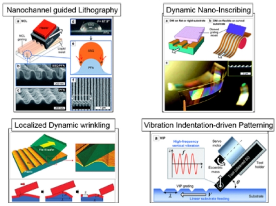
Jong. G Ok 교수 연구팀은 마스터몰드를 생산하기 위한 노력을 줄이고 이웃한 패턴 영역간 이음선을 없애기 위해 새로운 패터닝 기법 네가지를 개발하였다.
7-10 Fig. 3에 소개된 네가지 패터닝 기법은 물리적인 접촉에 기반한 패터닝 방법으로 최소화된 마스터 몰드 형상으로 2D 혹은 Quasi-3D 구조를 생산할 수 있다. Nanochannel Guided Lithography (NCL)와 Dynamic Nano-Inscribing (DNI)은 경질의 마스터 몰드를 활용하여 연질의 기판을 긁어내는 방식으로 미세구조를 형성하는 기술이다. 연속적으로 긁어내는 방식이기 때문에 대면적의 마스터 몰드 없이 길이방향으로 연속적인 라인 패턴이 형성될 수 있다. 패턴의 형상은 사용한 마스터 몰드와 기판의 탄성계수와 공정 시 가해진 하중, 공정 온도, 기판의 이송속도 등으로 결정되며 직선형태 뿐만아니라 곡선, 곡면상 패터닝, 꺾인 선 등도 자유롭게 표현 할 수 있는 장점이 있다. 특히, NCL은 이러한 각인 공정에 자외선 경화성 고분자를 도포하여 공정을 진행하기 때문에 DNI 대비 고종횡비의 미세 구조를 제작할 수 있다. 또한 부분 경화 기술을 활용하면 계층구조까지도 제작할 수 있다. DNI 공정의 경우 마스터 재료와 각인되는 기판의 경도와 인성이 매우 중요한 공정변수라 할 수 있으며 공정 직후 패턴의 탄성 회복 영향에 따른 형상 변화가 어느 정도 있을 수 있으므로 이를 고려한 마스터 패턴의 디자인이 필요하다. NCL은 이러한 형상 변화는 어느정도 극복할 수 있지만 반면에 사용하는 자외선 경화성 고분자의 기판상에서의 젖음 특성을 고려하여 공정을 수행해야한다. 젖음성이 너무 좋게 되면 고분자 아랫부분으로 각인된 기판에 고분자가 확산되어(Wetting) 원하는 형태의 고종횡비 구조를 얻기 어렵다. 반면에 젖음성이 너무 떨어지게 되면 경화 전의 고분자가 몰드 쪽으로 젖어(Wetting) 패터닝이 불가능하다. 그렇기 때문에 공정에 재료들을 적용하기 위해서는 사용 재료의 표면 장력에 대한 정보를 확인할 필요가 있다.
Fig. 3Schematics of seamless micro/nano patterning methods7-10 (reproduced from ref. 7-10 with permission)

Vibrational Indentation-Driven Patterning (VIP) 공정은 상기 언급한 두 기술과는 달리 주기적인 찍힘 현상을 활용하여 미세패턴을 생성한다. DNI 기술과 마찬가지로 마스터와 기판의 경도와 인성이 매우 중요한 공정변수이고 공정 온도와 기판의 이송속도 및 마스터의 진동속도에 따라 패턴의 크기와 형상이 변화한다. 이 기술은 실시간으로 패턴의 크기와 주기를 조절할 수 있는 장점이 있어 다양한 응용이 기대된다. Localized Dynamic Wrinkling (LDW)은 평평한 기판 둘이 마찰을 일으킬 때 연질면이 소성변형을 하면서 국부적인 주름이 생기는 현상을 활용한 패턴 기법이다. 이 기술 역시 특별한 마스터가 필요하지 않으며 최소 120 nm 크기의 패턴까지 구현할 수 있다. 다만 비교적 패턴 구현을 위한 연질 막 재료 선택의 폭이 좁아 실사용을 위해서는 주의 깊은 공정 설계가 필요하다.
상기 네 기술은 마스터 제작을 위한 복잡한 공정이 필요하지 않고 이음선이 없는 구조를 연속적으로 제작할 수 있기 때문에 적절한 응용처에서는 매우 높은 활용성을 지닐 것으로 예상된다. 하지만 라인 패턴이 아닌 고종횡비의 기둥 구조나 Quasi-3D 구조를 자유롭게 형성하는 것은 공정 특성상 불가능하다. 즉, NIL의 단점을 보완할 수 있는 기술이라기 보다는 NIL과는 또 다른 개념의 공정 기술로 접근하는 것이 적합할 것이다.
2.3 시각적 관용성을 갖는 타일링 기법
기존에 개발된 R2RNIL의 장점을 그대로 가져오면서 이음선에 의한 응용 한계를 없애기 위해서는 이음선 없는 몰드를 제작하는 기술이 필요하다.
M. Kwak 교수 그룹은 이러한 문제점을 해결하기 위해 시각적 관용성을 갖는 미세구조 타일링 패터닝 기술(Visually Tolerable Tiling, VTT)을 개발하였다.
11 이 기술은 기존의 타일링 기법에서 이웃한 패턴 영역간 간격을 겹칠 수 있는 정도까지 좁혀 이음선 자체를 시각적으로 인지하기 힘든 수준(~ 500 nm)까지 낮추어 패터닝 하는 것으로 적절한 재료의 선택과 공정 압력의 선정이 매우 중요한 공정 변수이다. VTT 공정의 실현을 위해 자가복제가 가능한 polyurethaneacrylate (PUA)를 패터닝 고분자로 사용하였고 기판으로는 PET 필름을 사용하였다.
23 경화된 PUA 패턴 위에서 경화되기전의 PUA 액상 고분자는 음수의 확산계수(Spreading Coefficient)를 가지면서 일정 수준의 젖음 후 확산을 멈추게 된다.
26 이 상태를 활용하여 반복적인 몰딩을 진행하게 되면 반복적으로 PUA 패턴들이 쌓이게 되는데 이때 적절한 공정압력에 의한 PUA 고분자의 불연속 이음선의 폭 및 높이가 500 nm 이하로 형성되면서 눈으로 확인 되지 않는 대면적 패턴이 완성된다.
27 Fig. 4는 이 공정을 나타낸 모식도이고
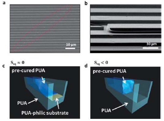
Fig. 5는 이 공정을 통해 제작된 마이크로구조 이음선 부분의 SEM 이미지와 고분자의 젖음 특성에 따른 확산에 대한 모식도이다. VTT 공정은 성공적인 패턴 면적 확장을 위해 고분자 도포의 적절한 양과 위치 그리고 적당한 세기의 가압이 중요하다. 너무 적은 양의 고분자는 충분한 확산이 되지 않아 이웃한 패턴 영역과의 겹친 부분을 만들어 낼 수 없다. 또한 너무 많은 양의 고분자는 마스터 몰드 영역을 넘어서까지 레진이 확산되면서 원치 않는 결점(Defects)을 남기게 된다. 즉, 적절한 양과 위치로 고분자가 도포될 때 효과적인 VTT 공정이 수행될 수 있다. 가압의 경우 너무 낮은 압력을 통한 공정은 두꺼운 레이어의 패턴을 남기기 때문에 시각적으로 이음선이 보이게 되고 너무 높은 압력을 통해 공정을 수행하게 되면 패턴형상이 무너지거나 패턴 전면적에 원치 않는 불규칙한 변형을 가져오게 되어 결과물의 완성도가 떨어진다. 이러한 공정의 완성도 향상을 위한 후속 연구는 VTT 자동화 장치의 개발과 공정 변수 연구를 통해 수행 중이다.
Fig. 4Schematics of visually tolerable tiling method and R2RNIL11 (reproduced from ref. 11 with permission)
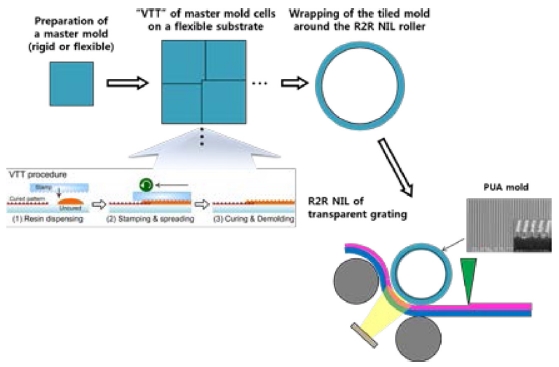
Fig. 5(a) SEM image of the seam part of micro-prismpatterns. (b) SEM image of step on the overlapped micro-gratings along the seam line. (c) Illustrations of complete wetting conditions with almost zero value of spreading coefficient. (d) Illustrations of partial wetting conditions with negative spreading coefficient11 (reproduced from ref. 11 with permission)
2.4 대표적 응용분야
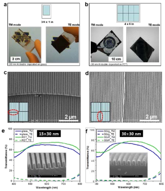
VTT 공정을 이용한 대면적 패턴은 R2RNIL 공정에서 롤타입 몰드로 사용될 수 있다. 이 기술을 활용하면 기존의 공정으로 제작할 수 없었던 고해상도 대면적 패턴을 저비용으로 간단히 제작할 수 있다. 대표적인 응용으로 대면적 Wire Grid Polarizer 제작에 본 기술을 적용하였다.
11 Figs. 6(a)와
6(b)는 VTT 기술 적용전의 소면적 마스터 몰드와 수십번의 반복 VTT 패터닝 후의 대면적 패턴의 이미지를 나타낸다.
Fig. 6(b)는 약 70 nm의 선폭을 갖는 높은 밀도의 라인패턴을 24 in
2의 면적에 걸쳐 잘 복제 한 결과를 보여준다. 사용한 복제 재료인 PUA는 자가복제 기능이 있기 때문에 한번의 VTT 공정을 통한 대면적 몰드의 제작을 통한 새로운 몰드의 생성은 연속적인 자가 복제를 가능케 하여 한번의 대면적 몰드 생산이후의 생산성을 비약적으로 높여준다.
23 비록 현재까지 개발된 VTT 공정은 매우 높은 숙련도가 요구되고 수율이 높지는 않지만 이러한 자가 복제 특성 덕분에 충분히 다양한 분야에서 활용될 수 있을 만한 잠재력을 지닌다 할 수 있다.
Figs. 6(c)와
6(d)는 VTT 공정을 진행한 패턴간의 경계면에서의 이음선을 보여주는 SEM 이미지이다. SEM 이미지 상에서는 분명히 불연속 이음선이 존재하지만 그 크기가 매우 작아 (~500 nm) 눈으로 샘플을 관찰하였을 때에는 그 경계가 잘 보이지 않는다. 이는
Fig. 6(b)에서 확인 할 수 있다. 편광효과 확보를 위해 VTT를 이용하여 복제된 넓은 면적의 나노 라인 패턴에 경사증착을 통해 Al을 증착하였다. 양쪽에 각기 다른 두께로 증착한 샘플의 편광특성을
Figs. 6(e)와
6(f)에 나타내었다. 증착한 Al의 두께에 따라 조금은 다른 광학적 특성을 나타내고 있지만 가시광 영역에서 대동소이한 편광 특성을 보여줌을 알 수 있다. 이 응용 예를 바탕으로 대면적의 샘플 제작시 결점의 유무가 매우 중요한 디스플레이 부품 소재 영역에서 효율적으로 대면적의 고해상도 패턴을 제작하는데 VTT 기술을 적용한 R2RNIL 기술이 활용될 수 있음을 확인할 수 있다. 이 밖에도 VTT 기술은 Moth Eye를 모사한 무반사 필름의 제작과 디스플레이 장치에 들어가는 프리즘 시트의 대면적화에도 활용되고 있다.
Fig. 6(a) Photo images of TE and TM modes of the fabricated wire grid polarizer with original master size. (b) TE and TM mode images of the large area wire grid polarizer which was fabricated by VTT. Large area sample was made by eight times overlapped patterning. All samples in (a) and (b) were fabricated by 30 + 30 nm double side deposition. (c, d) SEM images of seam part of nano-wire grid polarizer patterns. (e, f) cross-sectional SEM images and performance data of the 15 + 30 nm and 30 + 30 nm double side deposited wire grid polarizer11 (reproduced from ref. 11 with permission)
VTT 기술은 R2RNIL에 적용되어 생산성 향상을 위한 충분한 기여를 하고 있다. 향후 더욱 효율적인 VTT 기술의 활용을 위해 VTT 공정에 관계되는 공정 변수의 정량화와 장비 개발을 통한 자동화 기술이 필요할 것으로 예상된다.
3. 연속형 포토리소그래피
3.1 R2R Phase Shift Lithography
Phase Shift Lithography(위상반전리소그래피, PSL)는 규칙적인 작은 패턴을 빛이 통과할 때 발생하는 회절 현상을 이용한 패터닝 방법으로 특정 높이로 구현된 투명한 마스크를 사용한다.
13 특정 높이의 구조 기반 마스크를 사용하므로 NIL을 이용한 미세구조 샘플을 PSL의 마스크로 활용할 수 있다. 1998년 Whiteside 교수 연구진은 PDMS 마스크를 사용한 90 nm 선폭의 패턴을 성공적으로 생산하였다.
28 문헌에서 사용된 Polydimethylsiloxane (PDMS)은 자외선 영역에서 빛의 투과성이 좋고 전면적에 걸쳐 접촉이 매우 잘되므로 근접장(Near Field)에서 광학 회절 현상을 활용한 PSL에 적용하기 매우 유리하다. 이후 2004년 S. W. Jeon 교수 연구진은 같은 원리의 리소그래피 기술을 활용하여 복잡한 형태의 3D 나노 구조물을 제작하였고 이를 필터나 메타물질로 활용한 결과를 발표하였다.
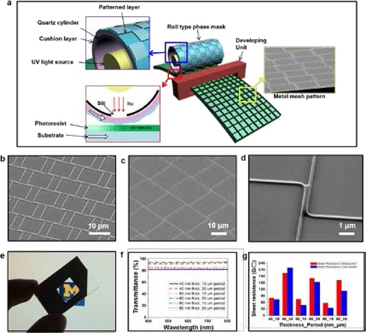
29,30 2011년 L. Jay Guo 교수 연구진은 이 기술에 대한 연속화를 연구하였고 롤형태의 마스크를 활용하여 PSL의 연속화에 성공하였다.
13 Fig. 7(a)는 롤타입 PSL의 공정 모식도를 나타낸다. 이 연구에서는 롤타입 PSL마스크로 PDMS 대신 PUA 기반의 고분자 마스크를 사용하였고 연속적이고 안정적인 접촉을 확보하기 위하여 쿠션층을 쿼츠롤과 PUA 몰드 사이에 적용하였다.
Fig. 7(a) Schematic illustration of R2R phase shift lithography (b) SEM image of Dense mesh pattern fabricated by R2RPSL (c) SEM image of Sparse mesh pattern (d) Enlarge SEM image of connection part (e) Photo image of fabricated transparent electrode (f) Transmittance of sample in e. (g) Sheet resistance of sample in e13 (reproduced from ref. 13 with permission)
PSL의 구현을 위해 패턴의 모서리에서 빛의 투과를 막으려면 정확히
π 만큼의 위상 변화가 필요하다.
28 이러한 위상변화를 구현하기 위해서는 마스크로 제작된 미소패턴의 높이가 중요한데 이는 사용된 빛의 파장과 마스크 물질의 굴절율로 구할 수 있다.
31
상기 식은 π 만큼의 위상 변화를 유도하기 위한 광원의 파장과 마스크 물질의 굴절률로 표시한 마스크 구조의 높이를 나타낸다. 이 연구에서는 375 nm의 자외선을 사용하였고 이에 따른 패턴의 높이는 375 nm에 맞추어 제작되었다. (PUA의 굴절률은 약 1.5) 개발한 연속 PSL 공정은 평면상의 패터닝과는 달리 롤타입의 마스크와 포토레지스트가 도포된 기판이 선접촉을 하기 때문에 효과적인 위상반전을 구현하기 위하여 적당한 가압으로 국부적인 평면을 만들어 연속적인 PSL 공정이 가능하게 되었다. 이 때문에 PDMS 패턴의 단일 사용보다는 쿠션층과 비교적 탄성계수가 높은 물질(예를들어 PUA)의 동시 사용이 추천된다. 연속 PSL을 사용하여 200 nm의 선폭을 갖는 라인패턴을 성공적으로 제작하였고 연속적으로 노광 공정을 할 수 있음을 보였다. 물론 PR 코팅과 현상(Develop)공정은 수동으로 진행하였지만 간단한 장치 추가로 연속화 및 자동화를 할 수 있는 가능성을 확인하였다.
이 장치를 활용한 응용 예로 메쉬 형태의 투명전극을 제작하였다.
Figs. 7(b)와
7(c)는 SEM 이미지는 다른 주기를 갖는 투명전극 샘플을 나타낸다. 마스크 패턴의 모서리를 따라 폐곡선으로 형성되는 PSL 공정의 특성을 감안하여 약간씩 겹쳐진 체커보드 형태의 마스크를 활용하여 연결된 나노 라인 금속 패턴을 제작하였다. 그 결과 높은 투과도와 낮은 면저항을 갖는 투명전극이 제작되었는데 기존에 널리 활용되고 있는 ITO와 비교하여 나쁘지 않은 수준의 성능을 보여주었다(
Figs. 7(e),
7(f),
7(g)).
롤타입의 포토리소그래피는 M. Kwak 교수 연구진에 의해 개발되었다.
32-34 이 기술은 기존 평면 기판형 포토리소그래피와 공정의 기본 원리를 공유하는데, 유일한 다른점은 유리기판위에 증착된 크롬층을 패터닝 하여 사용한 평면 포토마스크 대신 유연한 필름 위에 구현된 포토마스크를 사용한다는 점이다.
3 유연 포토마스크는 필름에 금속을 증착한 후 포토리소그래피나 NIL, E-Beam 리소그래피 등의 방법으로 제작한다. 제작된 유연 포토마스크는 기판과의 균일한 접촉과 부분적인 평면화를 이끌어내기 위해 쿠션층을 한층 설치한다음 쿼츠 롤에 부착된다.
Fig. 8(a)는 롤타입 포토리소그래피 공정의 모식도이다. PR 코팅된 기판이 롤형태의 마스크 노광장치 아래를 지나가면서 노광이 되고 이어 현상을 거치며 미세 구조가 제작된다. 앞서 다룬 R2RPSL과 마찬가지로 이 연구 역시 연속 노광에 대한 기술만 다루고 있어 상용화를 위해서는 PR 코팅과 현상에 대한 자동화 기술과 장치가 필요하다. 이 기술은 기본적으로 기존의 포토리소그래피 공정과 동일하지만 롤타입 공정 특성상 부가적인 기능이 존재한다. 마스크 형상의 일대일 전사만 할 수 있는 일반적인 포토리소그래피와는 달리 롤타입 포토리소그래피 공정은 기판과 접촉상태에서 완벽한 동조를 이루며 패터닝이 되는 방식과 비접촉 상태에서 속도의 차이를 두고 마스크 상의 패턴을 왜곡하여 기판에 표현하는 방식의 두가지 패터닝 공정이 있다.
Fig. 8(a) Schematic illustration of R2R photolithography (b) SEM image of fabricated metal mesh patterns with various periods (c) Sheet resistance of fabricated transparent electrodes (d) Transmittance of fabricated transparent electrodes3 (reproduced from ref. 3 with permission)
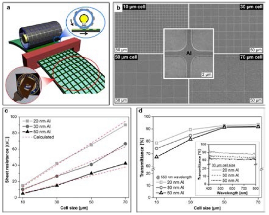
즉, 기판 이송속도 대비 롤마스크의 회전속도를 조절함으로써 패턴의 크기를 줄이거나 늘릴 수 있다. 이를 활용하면 하나의 마스크로 다양한 주기의 미소 패턴을 제작할 수 있다.
이 연구에서는 롤타입 포토리소그래피를 활용한 응용 예로 투명전극을 제작하였다. 금속 메쉬형태의 미세구조 제작을 통해 투과도와 면저항을 측정하여 투명전극으로서 가장 좋은 성능을 발휘할 수 있는 최적의 패턴 크기와 금속층의 증착 두께를 찾아냈다. 문헌에 따르면 면저항은 금속층의 두께가 높을수록 낮아지는 반면 투과도는 일정 크기 이상의 메쉬에서는 두께에 상관없이 일정하게 나타나기 때문에 기존의 ITO보다 훨씬 성능이 좋은 투명전극이 제작될 수 있었다.
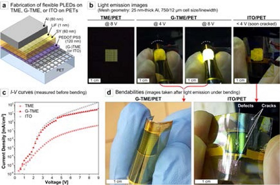
이렇게 제작된 메쉬형태의 투명전극은 금속의 인성이 ITO보다 훨씬 뛰어나기 때문에 유연한 전극으로서 더욱 활용도가 높다. 이에 대한 활용성을 테스트하기 위해 금속 메쉬 투명전극을 유연 PLED 소자의 전극으로 적용하여 굽힘 테스트를 수행하였고 그 결과 결점과 갈라짐이 발생한 ITO 사용 소자 대비 매우 안정적인 굽힘 안정성을 보여주었다(
Fig. 9).
Fig. 9(a) Schematic illustration of PLED device (b) Light emission test of various PLED devices with bending (c) I-V curve of PLEDs (d) Images of bending test result3 (reproduced from ref. 3 with permission)

이 외에도 롤타입 포토리소그래피는 기존의 포토리소그래피가 적용되는 분야에 자연스럽게 적용될 수 있다. 예를들어 현재 롤타입 포토리소그래피 공정은 Narrow Bezel 제작 분야와 PCB 기판 처리 분야에 적용되고 있고 그 영역을 확장하고 있다.
4. 결론
대표적인 마이크로/나노 구조의 제작기법인 포토리소그래피와 나노임프린트 리소그래피는 생산성을 높이기 위한 진화를 계속해 왔다. 포토리소그래피는 자동화 장비를 이용한 로봇 기반의 생산자동화를 이루었고 나노임프린트 리소그래피는 롤타입 공정의 개발로 연속 생산을 실현하였다. 최근 보다 높은 생산성을 달성하기 위해 포토리소그래피의 연속화와 나노임프린트 리소그래피의 대면적화가 진행되었고 이를 통한 생산 효율의 증대가 실현되었다. 이 과정에서 새로운 컨셉의 패터닝 기법도 개발되었고 기존 기술로는 구현하기 어려웠던 패턴도 비교적 쉽게 제작할 수 있게 되었다. 이 리뷰 논문에서는 포토리소그래피와 나노임프린트 리소그래피가 연구실의 기술개발 차원을 넘어 산업계에서 활발하게 사용될 수 있는 기술로 한걸음 다가선 기술 개발 동향을 다루었다. 관련 기술의 상용화를 위해서는 지난 20년간 많은 진보가 있었지만 여전히 많은 기술 개발이 필요하다. 본 리뷰 논문은 향후 관련 기술의 개발에 있어 좋은 방향을 설정을 할 수 있도록 관련 기술의 개발 동향과 기술의 장단점을 제시하였다. 상기 소개된 기술들은 추후 양산 적용 시 수율 향상을 위한 부가 기술의 개선이 있다면 근시일 내에 상용화 공정으로 활용될 수 있으리라 생각한다.
ACKNOWLEDGMENTS
이 논문은 2017학년도 경북대학교 연구년교수연구비에 의하여 연구되었습니다.
REFERENCES
- 1.
Chou, S. Y., Krauss, P. R., and Renstrom, P. J., “Imprint Lithography with 25-Nanometer Resolution,” Science, Vol. 272, No. 5258, pp. 85-87, 1996.
10.1126/science.272.5258.85
- 2.
Guo, L. J., “Nanoimprint Lithography: Methods and Material Requirements,” Advanced Materials, Vol. 19, No. 4, pp. 495-513, 2007.
10.1002/adma.200600882
- 3.
Ok, J. G., Kwak, M. K., Huard, C. M., Youn, H. S., and Guo, L. J., “Photo–Roll Lithography (PRL) for Continuous and Scalable Patterning with Application in Flexible Electronics,” Advanced Materials, Vol. 25, No. 45, pp. 6554-6561, 2013.
10.1002/adma.201303514
- 4.
Ahn, S. H. and Guo, L. J., “Large-Area Roll-to-Roll and Roll-to-Plate Nanoimprint Lithography: A Step Toward High-Throughput Application of Continuous Nanoimprinting,” ACS Nano, Vol. 3, No. 8, pp. 2304-2310, 2009.
10.1021/nn9003633
- 5.
Ok, J. G., Youn, H. S., Kwak, M. K., Lee, K. T., Shin, Y. J., et al., “Continuous and Scalable Fabrication of Flexible Metamaterial Films Via Roll-to-Roll Nanoimprint Process for Broadband Plasmonic Infrared Filters,” Applied Physics Letters, Vol. 101, No. 22, Paper No. 223102, 2012.
10.1063/1.4767995
- 6.
Yi, H., Hwang, I., Lee, J. H., Lee, D., Lim, H., et al., “Continuous and Scalable Fabrication of Bioinspired Dry Adhesives Via a Roll-to-Roll Process with Modulated Ultraviolet-Curable Resin,” ACS Applied Materials & Interfaces, Vol. 6, No. 16, pp. 14590-14599, 2014.
10.1021/am503901f
- 7.
Ahn, S. H. and Guo, L. J., “Dynamic Nanoinscribing for Continuous and Seamless Metal and Polymer Nanogratings,” Nano Letters, Vol. 9, No. 12, pp. 4392-4397, 2009.
10.1021/nl902682d
- 8.
Ahn, S. H. and Guo, L. J., “Spontaneous Formation of Periodic Nanostructures by Localized Dynamic Wrinkling,” Nano Letters, Vol. 10, No. 10, pp. 4228-4234, 2010.
10.1021/nl102694a
- 9.
Ahn, S. H., Ok, J. G., Kwak, M. K., Lee, K. T., Lee, J. Y., et al., “Template Free Vibrational Indentation Patterning (VIP) of Micro/Nanometer Scale Grating Structures with Real Time Pitch and Angle Tunability,” Advanced Functional Materials, Vol. 23, No. 37, pp. 4739-4744, 2013.
10.1002/adfm.201300293
- 10.
Ok, J. G., Park, H. J., Kwak, M. K., Pina Hernandez, C. A., Ahn, S. H., et al., “Continuous Patterning of Nanogratings by Nanochannel Guided Lithography on Liquid Resists,” Advanced Materials, Vol. 23, No. 38, pp. 4444-4448, 2011.
10.1002/adma.201102199
- 11.
Kwak, M. K., Ok, J. G., Lee, S. H., and Guo, L. J., “Visually Tolerable Tiling (VTT) for Making a Large-area Flexible Patterned Surface,” Materials Horizons, Vol. 2, No. 1, pp. 86-90, 2015.
10.1039/C4MH00159A
- 12.
Ahn, S. H. and Guo, L. J., “High?Speed Roll?to?Roll Nanoimprint Lithography on Flexible Plastic Substrates,” Advanced Materials, Vol. 20, No. 11, pp. 2044-2049, 2008.
10.1002/adma.200702650
- 13.
Kwak, M. K., Ok, J. G., Lee, J. Y., and Guo, L. J., “Continuous Phase-Shift Lithography with a Roll-Type Mask and Application to Transparent Conductor Fabrication,” Nanotechnology, Vol. 23, No. 34, Paper No. 344008, 2012.
10.1088/0957-4484/23/34/344008
- 14.
Khan, S., Lorenzelli, L., and Dahiya, R., “Technologies for Printing Sensors and Electronics Over Large Flexible Substrates: A Review,” IEEE Sensors Journal, Vol. 15, No. 6, pp. 3164-3185, 2014.
10.1109/JSEN.2014.2375203
- 15.
Krebs, F. C., “Fabrication and Processing of Polymer Solar Cells: A Review of Printing and Coating Techniques,” Solar Energy Materials and Solar Cells, Vol. 93, No. 4, pp. 394-412, 2009.
10.1016/j.solmat.2008.10.004
- 16.
Leigh, S. J., Bradley, R. J., Purssell, C. P., Billson, D. R., and Hutchins, D. A., “A Simple, Low-Cost Conductive Composite Material for 3D Printing of Electronic Sensors,” PloS One, Vol. 7, No. 11, Paper No. 49365, 2012.
10.1371/journal.pone.0049365
- 17.
Tate, J., Rogers, J. A., Jones, C. D., Vyas, B., Murphy, D. W., et al., “Anodization and Microcontact Printing on Electroless Silver: Solution-Based Fabrication Procedures for Low-Voltage Electronic Systems with Organic Active Components,” Langmuir, Vol. 16, No. 14, pp. 6054-6060, 2000.
10.1021/la991646b
- 18.
Wang, X., Jiang, M., Zhou, Z., Gou, J., and Hui, D., “3D Printing of Polymer Matrix Composites: A Review and Prospective,” Composites Part B: Engineering, Vol. 110, pp. 442-458, 2017.
10.1016/j.compositesb.2016.11.034
- 19.
Chou, S. Y., Krauss, P. R., Zhang, W., Guo, L., and Zhuang, L., “Sub-10 nm Imprint Lithography and Applications,” Journal of Vacuum Science & Technology B: Microelectronics and Nanometer Structures Processing, Measurement, and Phenomena, Vol. 15, No. 6, pp. 2897-2904, 1997.
10.1116/1.589752
- 20.
Chou, S. Y. and Krauss, P. R., “Imprint Lithography with Sub-10 nm Feature Size and High Throughput,” Microelectronic Engineering, Vol. 35, Nos. 1-4, pp. 237-240, 1997.
10.1016/S0167-9317(96)00097-4
- 21.
Colburn, M., Grot, A., Amistoso, M. N., Choi, B. J., Bailey, T. C., et al., “Step and Flash Imprint Lithography for Sub-100-nm Patterning,” Emerging Lithographic Technologies IV, pp. 453-458, 2000.
10.1117/12.390082
- 22.
Choi, J., Nielsch, K., Reiche, M., Wehrspohn, R., and Gösele, U., “Fabrication of Monodomain Alumina Pore Arrays with an Interpore Distance Smaller than the Lattice Constant of the Imprint Stamp,” Journal of Vacuum Science & Technology B: Microelectronics and Nanometer Structures Processing, Measurement, and Phenomena, Vol. 21, No. 2, pp. 763-766, 2003.
10.1116/1.1556397
- 23.
Choi, S.-J., Kim, H. N., Bae, W. G., and Suh, K.-Y., “Modulus- and Surface Energy-Tunable Ultraviolet-Curable Polyurethane Acrylate: Properties and Applications,” Journal of Materials Chemistry, Vol. 21, No. 38, pp. 14325-14335, 2011.
10.1039/c1jm12201k
- 24.
Haatainen, T., Majander, P., Riekkinen, T., and Ahopelto, J., “Nickel Stamp Fabrication Using Step & Stamp Imprint Lithography,” Microelectronic Engineering, Vol. 83, Nos. 4-9, pp. 948-950, 2006.
10.1016/j.mee.2006.01.038
- 25.
Koo, N., Bender, M., Plachetka, U., Fuchs, A., Wahlbrink, T., et al., “Improved Mold Fabrication for the Definition of High Quality Nanopatterns by Soft UV-Nanoimprint Lithography Using Diluted PDMS Material,” Microelectronic Engineering, Vol. 84, Nos. 5-8, pp. 904-908, 2007.
10.1016/j.mee.2007.01.017
- 26.
Kim, P., Kim, H.-Y., Kim, J. K., Reiter, G., and Suh, K. Y., “Multi-Curvature Liquid Meniscus in a Nanochannel: Evidence of Interplay Between Intermolecular and Surface Forces,” Lab on a Chip, Vol. 9, No. 22, pp. 3255-3260, 2009.
10.1039/b911271e
- 27.
Watts, M., Little, M., Egan, E., Hochbaum, A., Johns, C., et al, “A Process for and Properties of Low Cost Wire Grid Polarizers,” Agoura Technology, 2013.
10.1117/12.2008924
- 28.
Rogers, J. A., Paul, K. E., Jackman, R. J., and Whitesides, G. M., “Using an Elastomeric Phase Mask for Sub-100 nm Photolithography in the Optical Near Field,” Applied Physics Letters, Vol. 70, No. 20, pp. 2658-2660, 1997.
10.1063/1.118988
- 29.
Jeon, S., Park, J.-U., Cirelli, R., Yang, S., Heitzman, C. E., et al., “Fabricating Complex Three-Dimensional Nanostructures with High-Resolution Conformable Phase Masks,” National Academy of Sciences , Vol. 101, No. 34, pp. 12428-12433, 2004.
10.1073/pnas.0403048101
- 30.
Lee, T. W., Jeon, S., Maria, J., Zaumseil, J., Hsu, J. W., et al., “Soft Contact Optical Lithography using Transparent Elastomeric Stamps and Application to Nanopatterned Organic Light Emitting Devices,” Advanced Functional Materials, Vol. 15, No. 9, pp. 1435-1439, 2005.
10.1002/adfm.200500109
- 31.
Rogers, J. A., Paul, K. E., Jackman, R. J., and Whitesides, G. M., “Generating ~ 90 Nanometer Features Using Near-Field Contact-Mode Photolithography with an Elastomeric Phase Mask,” Journal of Vacuum Science & Technology B: Microelectronics and Nanometer Structures Processing, Measurement, and Phenomena, Vol. 16, No. 1, pp. 59-68, 1998.
10.1116/1.589836
- 32.
Lee, S. H., Kim, S. W., Park, C. W., Jeong, H. E., Ok, J. G., et al., “Scalable Fabrication of Flexible Transparent Heaters Comprising Continuously Created Metallic Micromesh Patterns Incorporated with Biomimetic Anti-Reflection Layers,” International Journal of Precision Engineering and Manufacturing-Green Technology, Vol. 4, No. 2, pp. 177-181, 2017.
10.1007/s40684-017-0022-1
- 33.
Lee, S. H., Lee, J. H., Park, C., and Kwak, M. K., “Roll-Type Photolithography for Continuous Fabrication of Narrow Bus Wires,” Journal of Micromechanics and Microengineering, Vol. 26, No. 11, pp. 115008, 2016.
10.1088/0960-1317/26/11/115008
- 34.
Lee, S. H., Lee, J. H., Park, C. W., Lee, C. Y., Kim, K., et al., “Continuous Fabrication of Bio-Inspired Water Collecting Surface Via Roll-Type Photolithography,” International Journal of Precision Engineering and Manufacturing-Green Technology, Vol. 1, No. 2, pp. 119-124, 2014.
10.1007/s40684-014-0016-1
Biography
- Moon Kyu Kwak
Associate Professor in the School of Mechanical Engineering, Kyungpook National University. His research interest is Micro/Nano fabrication and related applications.