ABSTRACT
We introduce technological development of stencil lithography, for new micro and nano fabricated method as a patterning technique. Stencil lithography has advantages of photoresistless, reusable patterning technique, and large area micro and nano patterning. The principle of stencil lithography is as follows: Materials are deposited through perforated holes on the membrane surface, of stencil in micro and nanoscale. In this paper, the fabrication method and application of three types of stencils, are reviewed according to the material. Solid-state stencils based on silicon, are fabricated by micro-fabrication processing of photolithography and etching. Metal stencils are fabricated by metal etching, electroforming, and laser machining. Polymer stencils are fabricated by molding and casting of polymers, such as PDMS, Hydrogel and Photocrosslinkable polymer, etc. Stencils fabricated from a variety of ways may be applied to nanopatterns, nano-wire patterning, and metal electrode fabrication, and used in metal deposition or etching masks and non-planar surface metal patterning techniques. Stencil lithography is applied in various areas of flexible displays, bio-devices, wearable sensors, etc.
-
KEYWORDS: Stencil lithography, Microstencil, Nanostencil, Micro-electro-mechanical systems, Shadow mask, Air-knife system
-
KEYWORDS: 스텐실 리소그래피, 마이크로스텐실, 나노스텐실, 초소형 정밀기계 기술, 섀도우마스크, 에어나이프 시스템
1. 서론
초소형 정밀기계기술의 하나인 MEMS (Micro-Electro Mechanical Systems)기술은 제품의 소형화, 고기능화, 직접화 등으로 다양하게 활용되고 있다. MEMS 제작에 필수적인 미세 패터닝과 미세 구조체 제작을 위하여 사용되는 포토리소그래피(Photolithography) 공정은 UV, Deep UV, X-ray, E-Beam 등의 광원을 이용하고 있다. 그러나 이들 기술들은 고가의 장비 사용과 재료 선택의 제한성 등의 한계가 존재하며 이를 극복하기 위한 새로운 미세 패터닝 기술 개발의 필요성이 요구되기 시작하였다.
1990년 후반 섀도우마스크(Shadow Mask)를 이용하여 원하는 물질을 표면 위로 직접 증착하는 스텐실 리소그래피(Stencil Lithography) 공정과 섀도우마스크 제작 기술에 관한 연구가 보고되면서 포토레지스트(Photoresist, PR) 없이 미세 패턴 제작이 가능한 새로운 패터닝 기술이 제안되었다.
1-10 이 기술은 모재와 증착 물질의 선택성이 높고, 고기능 바이오/화학 물질의 표면 패터닝이 용이하며, 기계적 강성이 약한 구조물의 패터닝에 활용이 가능한 장점을 가진다. 또한 공정의 간소화, 제조비용의 절감, 재사용 가능성, 광학기술 숙련의 불필요성 등 미세 패터닝 제조 기술에 많은 이점이 있다.
스텐실(Stencil), 또는 섀도우마스크는 종이, 나무, 금속, 폴리머 등의 얇은 막에 글자나 무늬, 그림 등 다양한 형상을 가지는 관통형 패턴을 만들고 그 안에 잉크를 넣어 찍어 내는 기법으로 인류 역사상 가장 오래된 기술들 중 하나이다. 스텐실을 나노/마이크로 공정으로 응용한 스텐실 리소그래피는 섀도우마스크 혹은 스텐실의 멤브레인(Membrane) 표면에 미리 정의 된 미세 패턴의 개방된 영역을 이용하여 원하는 물질을 동일한 크기와 형상으로 증착시키는 방법이다. 이러한 기술은 포토레지스트가 필요 없는 단일 공정으로 개방된 미세 패턴과 동일한 크기와 형상으로 전사가 가능하고, 포토리소그래피 공정인 PR 코팅(Spin Coating), 노광(Exposure), 현상(Development), 증착(Deposition), 식각(Etching) 및 리프트 오프(Lift-Off) 공정이 필요 없는 반영구적으로 사용이 가능하다. 또한 스텐실을 기판 위에 올려 패터닝 후 제거 할 수 있기 때문에 새로운 기판으로 연속 사용이 가능하므로 나노/마이크로 공정의 제조 비용이 절감되며, 미세 패터닝을 위한 복잡한 준비 시간이 줄어드는 장점을 가지므로 제조 공정의 생선성 증대에 큰 효과가 있다.
스텐실은 재료에 따라 세가지 유형으로 분류가 가능하다. 실리콘 웨이퍼(Slicon Wafer)와 질화실리콘(Silicon Nitride, SiN)을 기반으로 제작되는 실리콘 기반 스텐실,
1-10, 금속판을 직접 가공하거나 혹은 금속 증착을 이용하여 제작되는 금속 기반의 스텐실, MEMS 공정으로 제작된 마스터 몰드와 폴리머를 이용하여 가압(Pressure-Assisted), 마이크로 유체 채널(Microfluidic), 가스블로잉(Gas Blowing) 공정 등으로 제작되는 폴리머 기반의 스텐실로 분류된다. 이러한 스텐실은 재사용이 가능하고 제조비용과 시간을 크게 줄일 수 있는 장점을 가지며, 재료 특성에 따라 나노/마이크로 구조 제작 및 금속전극 패터닝, 디스플레이와 반도체 공정의 식각 및 증착용 마스크, 바이오 공학과 첨단 디스플레이 산업 등 다양한 분야로 활용 되고 있다.
본 논문에서는 재료의 성질에 따라 분류된 세가지 유형의 스텐실에 대하여 제작기법과 활용성에 관한 기술의 최근 연구 동향을 소개하고자 한다.
2. 스텐실 리소그래피 공정
일반적으로 실리콘 기반 MEMS 공정을 이용한 나노/마이크로 구조의 제작은 평평하고 단단한 기판(실리콘 웨이퍼) 위에 포토레지스트를 도포하여 포토리소그래피, 전자 빔 리소그래피(Electron-Beam Lithography, EBL)를 사용하여 포토레지스트 패턴을 만들고, 박막 증착 및 식각으로 제작한다. 이러한 기술은 나노/마이크로 구조 제작에 여러 공정이 필요하며 시간과 비용의 소모가 크다.
스텐실 리소그래피는 새로운 나노/마이크로 구조의 제작 기술로 공정이 간단하고 다양한 금속과 바이오/화학 물질을 사용할 수 있어 확장성이 우수하며 스텐실의 재사용이 가능한 장점을 가지는 제작 기술이다. 이 기술은
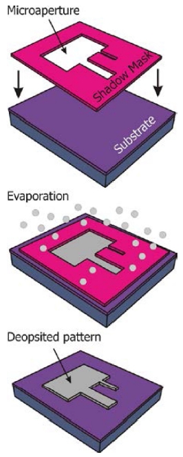
Fig. 1과 같이 스텐실을 이용하여 직접 원하는 물질을 표면 위에 증착하는 원리로 나노/마이크로 구조의 제작이 가능하다. 스텐실 리소그래피는 미세 패턴을 형성하고자 하는 표면 위에 미세 패턴이 개방된 스텐실을 고정하고 타겟물질을 물리적 또는 화학적으로 증착시켜 개방된 스텐실의 미세 패턴과 동일한 형태로 표면에 일대일로 전사가 된다. 이러한 방법은 증착 공정 후 스텐실을 제거하면 단일 공정으로 원하는 금속 물질을 증착할 수 있고, 공정이 진공 내에서 이루어지므로 표면 변질 및 건조 시 표면장력으로 인한 구조물의 표면 점착과 파괴 등 다양한 문제점들을 해결할 수 있다.
1,2
Fig. 1 Process of stencil lithography1 (Adapted from Ref. 1 on the basis of open access)

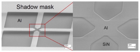
Fig. 2는 스텐실 리소그래피 공정을 이용하여 전자 빔 기화 증착(E-Beam Evaporation) 방법으로 알루미늄(Al)을 실리콘(Si)과 질화실리콘(SiN) 표면에 증착한 예를 보여주고 있으며, Kim et al.
1은 스텐실 제거 후 알루미늄 미세 패턴의 증착 결과를 원자력 현미경(Atomic Force Microscope, AFM)으로 표면 굴곡형상(Topography)을 측정 및 분석하여 알루미늄의 미세 패터닝이 가능함을 확인하였다.
Fig. 2 Shadowmask and evaporated surface after evaporation.of 100 nm thick Al layer1 (Adapted from Ref. 1 on the basis of open access)

스텐실 리소그래피 공정은 스텐실의 멤브레인에 정의된 미세패턴을 통하여 원하는 물질을 직접 증착시켜 단일공정으로 금속의 미세 패터닝이 가능하므로 공정의 단순화를 통한 효율성이 증대되고, 표면과 물질의 제약을 크게 완화할 수 있으며, 재사용이 가능하므로 공정단가를 낮출 수 있다.
3. 실리콘 기반의 스텐실
스텐실 리소그래피는 스텐실을 기판의 특정 위치에 배치하여 포토레지스트 없이 증착으로 마이크로 및 나노 구조를 패터닝하는 기술이며, 재료의 성질에 따라 세가지 유형으로
Fig. 3과 같이 분류할 수 있다. 그 중 실리콘(Si)과 질화실리콘(SiN) 같은 단단한 물질을 이용하여 제작되는 실리콘 기반 스텐실은 나노 리소그래피 공정으로 주로 활용된다(
Fig. 3(a)).
Fig. 3 Classification according to materials’ properties of stencil. (a) Silicon nanostencil, (b) Metal microstencil, (c) PDMS microstencil

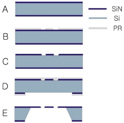
SiN는 열 안정성, 기계적 강도 및 화학적 불활성으로 인해 나노스텐실을 제작하기에 이상적인 소재이며 실리콘 웨이퍼 상에 증착된 저응력 SiN층에 전자 빔 리소그래피와 건식 식각(Dry Etching)으로 패턴을 정의하고 후면을 수산화칼륨(KOH) 용액을 이용하여 실리콘 웨이퍼를 직접 습식 식각(Wet Etching)하여 얇은 막 형태의 SiN 멤브레인을 제작한다.
1,2,4-12 제작된 SiN 멤브레인은 나노 크기의 패턴을 가진 증착용 마스크로 수십 - 수백 나노 크기의 금속 패턴 전사 및 금속 나노/마이크로 구조물을 제작하는데 활용되고 있다. 그리고 실리콘 웨이퍼를 증착용 마스크로 사용하기 위해 제작되는 실리콘 스텐실은 실리콘 웨이퍼에 산화실리콘(SiO
2)막에 패턴을 정의하고 DRIE (Deep Reactive Ion Etching)를 이용하여 실리콘을 가공한 후, 후면 연마공정을 통하여 실리콘 스텐실을 제작하여 금속 패턴 증착으로 사용된다.
3
실리콘 기반 스텐실의 제작은
Fig. 4와 같이 주로 저응력 SiN을 가공하여 제작된다. 양면 폴리싱 실리콘 웨이퍼에 저응력 SiN 막을 LPCVD (Low Pressure Chemical Vapour Deposition)로 증착하고 포토소그래피 공정을 이용하여 마스크 패턴을 형성한다. 그리고 ICP (Inductively Coupled Plasma) 식각으로 SiN 막을 제거하여 웨이퍼 윗면의 SiN 막 패턴을 형성한다. 뒷면의 SiN 막은 동일한 공정을 사용하여 계산된 크기를 가지는 마스크 패턴을 형성 후 KOH 용액으로 실리콘 식각(Bulk Silicon Etching)을 수행하여 SiN 멤브레인을 가지는 스텐실을 제작한다.
Fig. 4Fabrication process of silicon nitride (SiN) stencil. (a) Deposition of 500-nm-thick low stress SiN. (b) Photolithography of pattern. (c) SiN etching on front side. (d) Photolithography and SiN etching on backside. (e) KOH etching of bulk Si from backside for 500-nm-thick SiN membrane releasing
Bruger et al.
4는 벌크 마이크로머시닝(Bulk Micro-Machining) 기술을 사용하여 2 μm 크기를 가지는 실리콘 기반의 증착용 섀도우마스크를 제작하였다. Ootuka et al.
5는 200 nm 두께의 Si
3N
4 멤브레인을 나노스텐실 마스크로 사용하여 강자성 금속(Ferromagnetic Metal) 증착 공정으로 Ni/NiO/Co 터널 접합 어레이(Tunnel-Junction Array)를 제작하였다. 동일한 스텐실 제작 공정을 사용하여 Kohler et al.
6는 Si
3N
4 멤브레인을 증착용 마스크로 170 - 550 nm 크기를 가지는 크롬 패턴을 제작하였다. Deshmukh et al.
7는 전자 빔 리소그래피를 이용하여 마스크 패턴을 형성하고 CHF
3/O
2 플라즈마로 식각하여 나노스텐실을 제작하였다. 제작된 나노스텐실을 증착용 마스크로 사용하여 15 - 20 nm 폭을 가지는 금속 패턴을 제작하는 기술을 보고하였다. Brugger et al.
8는 LIL (Laser-Interferenc Lithography)과 식각 공정으로 나노스텐실을 제작하고 300 nm 크기의 단층 금속 패턴을 간단하고 저렴한 비용으로 제작하는 방법을 제안하였다. Kim et al.
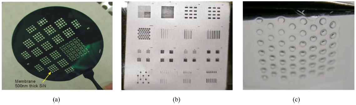
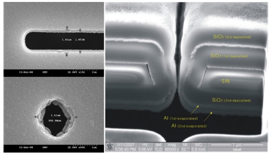
1은 실리콘 웨이퍼 전면에 388개 이상의 멤브레인을 가지는 나노스텐실을 저응력 SiN 막으로 제작하였으며, 국부 증착을 통하여 나노스텐실의 실효성을 검증하였다.
Fig. 5는 SiN 나노스텐실의 뒷면을 전자주사 현미경(Scanning electron microscopy, SEM)으로 확인한 사진으로 나노스텐실의 예를 보여주고 있다. Kim et al.
2,9,10은 일반적인 나노스텐실 제작공정에 집속 이온 빔(Forcused Ion Beam, FIB) 밀링을 결합하여 선폭 100 nm 이하의 나노스텐실을 제작하는 기술을 제안하고 국부증착으로 선폭 70 nm 크기의 극소형 나노패턴을 제작하였다. Tun et al.
11은 나노스텐실을 이용하여 20 - 100 nm 폭을 가지는 Au 나노와이어(Nanowire)를 증착하고 기판과 금속 나노와이어의 형상과 크기를 분석하는 연구를 수행하였다. Vazquez-Mena et al.
12는 미리 정의된 전기 패드를 갖는 기판에 Au/Al 나노와이어를 증착하여 와이어의 형태와 저항에 대한 연구를 수행하였다. 또한 100 mm 크기의 실리콘 웨이퍼 전체에 금속 나노와이어를 제작하는 기술을 보여주었다.
Fig. 5SEM image of a fabricated SiN nanostencil from the backside1 (Adapted from Ref. 1 on the basis of open access)

Kim et al.
3은 실리콘 웨이퍼와 산화막을 패터닝하고 실리콘 기판을 350 μm 정도 식각 후 후면을 연마하여 관통형 스텐실을 제작하는 방법을 제안하였다. 후면 연마공정을 사용하여 기존의 나노스텐실 제작 공정보다 단순하게 스텐실을 제작하였으며, 폭 45 μm 크기의 패턴을 가지는 실리콘 스텐실을 제작하여 금속 증착용 마스크로 사용하였다.
나노스텐실은 일반적으로 포토레지스트 없이 재사용이 가능하고 넓은 영역의 나노/마이크로 금속 구조의 제작과 패터닝으로 많이 활용되었다. 많은 연구자들은 실리콘 기반의 나노스텐실로 다양한 금속을 증착하는 연구를 수행하였다.
그러나 나노스텐실을 이용한 금속의 증착 공정에서 미세패턴의 막힘(Clogging) 현상과 미세패턴이 커지는 블러링(Blurring) 효과에 관한 문제점이 존재한다. 증착 공정에서 금속입자는 스텐실의 미세패턴을 수직 경로로 통과하여 대상 기판에 증착되지만 증착 각도의 변화로 스텐실 미세패턴 주위에 금속입자가 증착되어 막히는 현상이 발생하기도 한다. 또한 동일한 스텐실로 여러 번 패터닝을 하면 미세패턴에 금속입자가 증착되어 미세패턴의 크기가 감소되는 문제가 있다. 이러한 문제를 해결하기 위해 SAM (Self-Assembled Monolayer)을 이용하여 미세패턴 주변의 금속입자 접착을 감소시키는 방법과 습식 식각을 사용하여 금(Au) 및 알루미늄(Al)과 같은 금속입자를 제거하는 방법이 보고되었다.
Kolbel et al.
13,14는 나노스텐실을 SAM으로 코팅하여 증착 공정에서 나노스텐실의 개방형 패턴 막힘을 줄일 수 있음을 제안하였다. SAM 코팅 된 나노스텐실의 개방형 패턴에 금의 접착이 현저히 감소함을 실험을 통해 확인하였다.
나노스텐실을 이용한 금속 증착에서 미세패턴의 막힘 현상은 나노 크기를 가지는 미세패턴을 제작하기에 좋은 아이디어로 활용되었다. 나노스텐실의 미세패턴이 막힘 현상으로 인하여 패턴의 크기가 감소되므로
Fig. 6과 같이 증착 공정을 제어하면 원래의 미세패턴보다 작은 크기를 가지는 나노 패턴 제작이 가능하다.
Fig. 6SEM image of size tuning of apertures on nanostencil by additional deposition
Lee et al.
15는
Fig. 4와 같은 공정으로 나노스텐실을 제작하고 나노스텐실 표면에 이산화규소(SiO
2)를 PECVD (Plasma Enhanced Chemical Vapor Deposition)로 부가증착하여 나노 패턴의 선폭을 100㎚ 크기로 줄이는 연구를 수행하였다(
Fig. 6). 이러한 기술은 증착 방향과 방법에 따라 다양한 치수를 갖는 높은 종횡비 3D 나노 구조를 만드는데 사용이 가능하다.
일반적으로 스텐실 패터닝에서 스텐실과 대상 기판 사이의 갭(Gap)이 존재한다. 갭으로 인하여 금속입자가 개방형 패턴을 통해 기판으로 증착될 때 개방형 패턴보다 큰 크기를 가지는 패턴이 형성되는데 이를 블러링 효과라 한다. 블러링 효과가 나노 패턴의 크기를 확대하므로 패터닝 중 스텐실과 대상 기판 사이의 갭을 줄일 수 있는 기술에 관한 연구가 보고되었다.
Villanueva et al.
16는
Fig. 4와 같은 방법으로 나노스텐실을 제작하고 상이한 기판의 국부적 식각이 가능한 마스크로 활용하였다. 그리고 식각 공정에서 발생하는 스텐실과 대상 기판과의 갭 및 고정에 대한 문제점을 최소화하는 연구를 수행하였다. Sidler et al.
17는 순응형 박막(Compliant Membrane)을 사용하여 나노스텐실과 대상 기판의 갭을 줄여 블러링 효과를 95% 감소시키는 연구를 수행하였다.
실리콘 기반 나노스텐실의 연구는 증착을 이용한 금속 패터닝뿐만 아니라 다양한 분야로 응용되고 있다.
Özyilmaz et al.
18는 FIB를 이용한 나노스텐실로 자기성 나노 구조(Magnetic Nanostructure)를 제작하여 STT (Spin Transfer Torque) 연구로 응용하였다. Park et al.
19,20은 병렬 나노브릿지(Parallel Nanobridge) 패턴을 제작하기 위하여 SiN 나노스텐실, 가장자리 패터닝(Edge Patterning), 역나노스텐실 공정(Reverse Nanostencil Process)을 접목하여 85 nm 크기의 병렬 크롬(Cr) 나노 브릿지 패턴을 제작하였다. Du et al.
21는 나노스텐실을 크롬 증착용 마스크로 사용하여 마이크로 구조에 크롬 나노 패턴을 형성하고 이를 식각을 위한 마스크로 사용하여 DRIE (Deep Reactive Ion Etching)로 마이크로 구조 위에 선택적으로 고종횡비(High-Aspect-Ratio)를 가지는 나노/마이크로 복합 구조체를 제작하는 연구를 수행하였다. Agarwal et al.
22는 실리콘 스텐실의 개방된 패턴 사이의 두 전극 간격을 1 - 2 μm 크기로 제작하여 이를 분산된 단일벽 탄소나노튜브(Single-Walled Carbon Nanotubes, SWNTs)의 패터닝으로 응용하였다. Boogaart. et al.
23은 SiN 나노 스텐실을 증착용 마스크로 사용하기 위하여 유한요소법(FEM)과 실험결과 분석으로 멤브레인의 변형을 줄일 수 있는 안정화된 구조 설계에 관한 연구를 보고하였다.
4. 금속 기반의 스텐실
금속 기반의 스텐실(
Fig. 3(b))은 금속판의 개방된 미세 패턴을 이용하여 OLED와 같은 디스플레이 장치와 반도체 공정의 식각용 마스크 및 박막 증착용 마스크로 활용되며, 가공 방법에 따라 식각, 증착, 레이저 가공으로 분류된다. 산업용으로 많이 사용되는 금속 기반의 스텐실 제작 기법으로는 화학적 습식 식각(Chemical Wet Etching)을 이용하는 방법과 전주도금(Electroforming)을 이용한 금속 증착법 그리고 레이저(Laser)를 이용한 광학적 가공법이 많이 사용된다. 화학적 습식 식각 방식은 포토리소그래피 공정을 이용하여 금속판을 패터닝하고 금속의 선택적 식각을 위하여 금속 에첸트(Etchant)를 사용하여 제작한다. 에첸트는 금속판의 포토레지스트가 없는 부분의 금속만 등방성 식각하여 관통된 패턴을 형성하게 된다. 이러한 금속 스텐실 제작 공정에서 포토레지스트는 식각용 마스크로 사용되며 금속 스텐실 제작 후 포토레지스트는 제거된다. 전주도금을 이용한 금속 증착 방식은 포토리소그래피 공정으로 미세 패턴을 제작한 금속판에 전주도금의 통전 원리를 이용하여 원하는 패턴 부분만 선택적으로 도금하여 금속 스텐실을 제작하는 방법으로 니켈(Nickel), 구리(Copper), 니켈 코발트 합금(Nickel-Cobalt Alloy)등을 주로 사용하여 제작한다.
Fig. 3(b)는 니켈 전주도금을 이용하여 제작된 금속 스텐실의 예이다. 레이저 가공 방식은 금속판을 직접 가공하는 방법으로 고가의 레이저 장비를 이용하여 레이저 에너지의 흡수 조건을 조정하여 금속 기반의 스텐실을 제작한다.
이러한 금속 기반의 스텐실은 디스플레이 산업으로 활용되는 산업 기반 기술로 차세대 디스플레이 산업의 금속 패터닝, 플렉서블(Flexible), 웨어러블(Wearable) 기반의 전자 장치 제작, 바이오센서의 전극 패터닝 등으로 적용되고 있다. 또한 차세대 디스플레이 산업의 초미세화, 초정밀화, 대면적 양산을 통한 공정 단순화와 고품질화 등의 기반 기술로 활용되고 있다.
Chung et al.
24은 OLED (Organic Light Emitting Diode)와 같은 디스플레이 장치에 사용되는 Invar (Invariable Alloy) 합금 스텐실을 펨토초 레이저(Femtosecond Laser)를 이용하여 가공하는 연구를 수행하였다. Invar 합금 스텐실 가공에서 레이저 출력, 테이블 이송 속도와 깊이 방향 이송변화 등 실험 변수를 사용하여 깨끗한 가공면을 형성한 원형 모양을 구현하여 금속 기반의 스텐실 가공 가능성을 확인하였다.
Jeerapan et al.,
25 Malzahn et al.,
26 Mishra et al.
27는 스테인리스 강(Stainless Steel) 스텐실을 제작하여 전도성 잉크(Conductive Ink)를 이용한 플렉서블, 웨어러블 기반의 전자 장치 제작 및 바이오 센서의 전극을 패터닝하고 이를 차세대 디스플레이와 웨어러블 센서로 활용하는 연구를 수행하였다.
5. 폴리머 기반의 스텐실
폴리머 마이크로스텐실은 미리 정의된 패턴은 개방되어 있고 나머지 부분은 막혀있는 얇은 폴리머 멤브레인으로 재료의 성질에 따라 두 종류가 있으며, 생체적합성과 유연한 성질을 가지는 고분자인 폴리디메틸실록산(Polydimethylsiloxane, PDMS)을 이용한 PDMS 스텐실(
Fig. 3(C))과 광경화성(Photocrosslinkable) 폴리머를 이용한 하이드로젤(Hydrogel) 스텐실(
Fig. 11)이 있다. 이러한 폴리머 기반의 스텐실은 세포배양용 디바이스, 세포 패터닝으로 활용되는 바이오 공학 응용 및 플렉시블 디스플레이와 곡면 패터닝으로 활용되는 첨단 디스플레이 산업으로 많은 연구가 진행되고 있다.
PDMS는 화학적으로 안정한 특성을 가지는 폴리머로 강한 내구성과 유연한 특성으로 비평면 표면에 구조물 제작과 패턴 생성 및 마이크로 구조의 복제(Replication)로 사용되고 있으며, 광학적으로 투명한 성질을 이용한 광학장치로도 활용이 가능한 폴리머이다. 또한 PDMS는 독성이 없는 생체적합성 특성을 가지고 있기 때문에 생체연구 및 세포 배양을 위한 소형장치 제작으로 활발한 연구가 진행되고 있다.
Fig. 7은 PDMS 마이크로스텐실의 다양한 제작 방법들을 보여주고 있다.
Fig. 7(a) Fabrication of PDMS microstencil using microfluidic replication; (b) Fabrication of PDMS microstencil using pressure-assisted replication.; (c) Fabrication of PDMS microstencil using gas-blowing replication
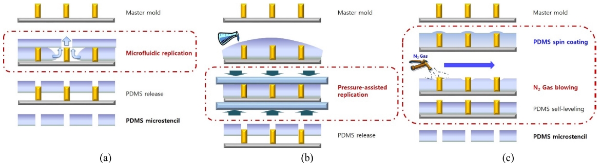
PDMS 마이크로스텐실의 가장 보편화된 제작 방법은 가압 공정과 마이크로 유체 채널을 이용한 흡입(Suction) 공정으로 Albert Folch와 그의 연구팀에 의해 제안되었다.
Folch et al.
28,29는 마이크로 유체 채널과 미세구멍에 연결된 주사기(Syringe)를 이용하여 미세구멍을 통해 PDMS를 흡입하여 PDMS 마이크로스텐실을 제작하는 방법(
Fig. 7(a))과 포토리소그래피로 제작한 마스터 몰드 위로 가압이 가능한 판을 눌러 압력을 이용하여 PDMS 마이크로스텐실을 제작하는 방법(
Fig. 7(b))을 사용하였다. 2000년에 보고된 이러한 제작 방법은 지금까지 많은 연구자들에 의해 사용되고 있다. Park et al.
30은 가압판을 이용하여 마스터 몰드 위 PDMS 중합체를 눌러서 제작하는 방법으로 100 μm, 300 μm, 500 μm 크기를 가지는 PDMS 마이크로스텐실을 제작하여 세포배양용 섀도우마스크로 활용하였다. 그리고 Cho et al.
31는 Park과 동일한 가압판 공정을 사용하여 550 μm 크기의 PDMS 마이크로스텐실을 제작하여 세포의 공동배양(Co-Cluture) 장치로 사용하였다. Hattori et al.
32은 가압 공정과 미세구멍을 통한 PDMS 흡입 방식의 단점을 보완하기 위하여 두 가지 공정을 결합하여 새로운 제작 방법으로 기존의 제작방법의 문제점을 해결하였다. Choi et al.
33는 가압 공정으로 PDMS 마이크로스텐실을 제작할 때 발생하는 10 - 20 μm 두께의 얇은 PDMS 막을 습식 식각으로 제거하여 다양한 패턴을 가지는 PDMS 마이크로스텐실을 제작하고 비평면 표면의 증착 및 식각용 섀도우마스크로 응용하였다. Li et al.
34는 가압 공정에서 발생하는 잔류 PDMS 막 제거를 플라즈마 에칭(Reactive Ion Etching, RIE)을 이용하여 해결하였으며, 3 μm 크기의 개방형 패턴을 가지는 관통형 PDMS 마이크로스텐실 제작이 가능함을 보였다.
최근에 보고된 가스블로잉 공정(
Fig. 7(c))을 이용한 PDMS 마이크로스텐실 제작은 마스터 몰드에 PDMS를 스핀코팅(Spin Coating)한 후 그 위로 질소가스(Nitrogen Gas)를 분사하여 마스터 몰드 위에 생성된 얇은 PDMS 막을 쉽게 제거하는 방법으로 가압이나 흡입을 위한 장치가 필요 없고 간단한 공정으로 관통형 패턴을 제작할 수 있다. 그리고 구조에 따라 단층구조의 스텐실과 이중구조의 스텐실 제작으로 응용이 가능하다.
Choi et al.
35는 가스블로잉 공정을 이용하여 PDMS 마이크로스텐실을 제작하는 방법을 제안하고,
Fig. 7(c)와 같은 공정을 사용하여 질소가스의 유량, 거리 등 다양한 실험변수를 조정하여 마이크로스텐실을 제작하였다. 그리고 Choi et al.
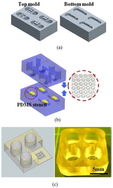
36는 동일한 공정으로 이중구조를 가지는 마이크로스텐실(Microwell Plate)을 제작하는 방법을 제안하였다.
Fig. 8은 아크릴 몰드(Acryl Mold)와 PDMS 마이크로스텐실을 결합하여 제작된 이중구조체 마이크로웰 플레이트로 높은 격벽과 구역분리가 가능한 다중구조체 제작이 가능함을 보여주는 예이다. 제작된 마이크로웰 플레이트는 신경세포의 마이크로 패턴 세포 배양 후 각각의 신경세포 패턴을 세포 분화로 활용하는 실험에 사용하였다.
Fig. 8Fabrication process of PDMS microwell plate and image (a) Machining of acryl mold for compartment, (b) Insertion of PDMS microstencil and PDMS casting, (c) Microwell plate
이러한 제작 방법 이외에 레이저 가공, 펀칭 등 다양한 방법을 사용한 PDMS 마이크로스텐실의 제작이 보고되었다.
Shiku et al.
37는 300 μm 크기의 원형 패턴을 가지는 PDMS 마이크로스텐실을 CO
2 레이저를 사용하여 PDMS를 직접 가공하여 스텐실을 제작하는 방법을 보여주었다. Raof et al.
38는 고가의 장비가 필요없는 간편한 제작 방법을 제안하였다. 1 mm 두께의 PDMS 필름에 외경이 500 μm 크기를 가지는 주사기 바늘로 펀칭하는 방법을 통해 550 μm 크기의 관통형 PDMS 마이크로스텐실을 쉽게 제작하였다. Nam et al.
39는 제거가 용이한 얇은 포토레지스 층에 PDMS를 스핀코팅으로 도포하여 마이크로스텐실을 제작하고 포토레지스트를 희생층으로 사용하여 얇은 PDMS 마이크로스텐실을 분리하는 방법을 제안하였다.
PDMS 마이크로스텐실은 다양한 방법으로 제작이 가능하지만 가스블로잉 공정의 기술적 한계인 숙련도에 의한 재현성과 마이크로스텐실 형상 제어 문제, 잔류 PDMS 막 제거를 위해 사용되는 고가의 플라즈마 에칭 장비의 사용, 흡입과 가압을 이용한 공정의 문제점인 외부장치 사용과 낮은 관통 수율 및 대면적과 대량생산의 어려움 등과 같은 단점을 가지고 있다. 이러한 단점을 극복한 새로운 자동화 시스템과 연속 생산 공정에 대한 연구가 최근 보고되었다.
Choi et al.
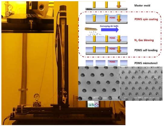
40가 제안한 에어나이프(Air-Knife) 시스템(
Fig. 9)을 이용한 자동생산 시스템은 대면적 제작이 가능하고 공정시간 단축을 통한 대량생산이 가능한 방법으로 숙련도의 영향이 없고 재현성이 높으며 누구나 쉽게 제작할 수 있다. 에어나이프 시스템을 이용한 자동생산 시스템은 자동 이송장치와 질소가스의 대면적 분사가 가능한 에어나이프로 구성되며 마스터 몰드의 잔류 PDMS 층을 대면적 분사를 통해 쉽고 빠르게 제거하는 방법으로 가스블로잉 기술의 단점을 극복한 새로운 형태의 자동화 공법이다. 그리고 Choi et al.
41는 에어나이프 시스템을 사용하여 3차원 복합 형상을 가지는 PDMS 마이크로스텐실을 제작하는 방법을 제안하고, 이를 3차원 세포배양기술로 적용하여 간세포를 3차원 입체형상으로 배양하는 In Vitro 세포연구를 수행하였다. Kim et al.
42은 에어나이프 시스템으로 PDMS 마이크로스텐실을 제작하고 스텐실의 미세패턴에 PLGA (Poly Lactic-Co-Glycolic Acid) 용액을 채워 용매증발(Solvent Evaporation) 방식과 결합한 응용연구로 PLGA 마이크로 컨테이너(Microcontainer)를 제작하여 세포 이송장치로 활용하였다.
Fig. 9Air-knife automation system and SEM image of PDMS microstencil

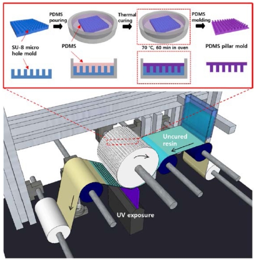
Fig. 10은 롤-투-롤(Roll-to-Roll) 임프린트 공정으로 PDMS 마이크로스텐실의 연속 생산이 가능한 시스템을 보여주고 있다. Lee et al.
43는 롤-투-롤 임프린트 장치에 미세패턴이 형성된 소수성(Hydrophobicity) PDMS 몰드와 친수성(Hydrophilicity)을 가지는 광경화성 PUA(Polyurethane Acrylate)의 비젖음(Dewetting) 현상을 이용하여 연속생산이 가능한 자동화 시스템을 제안하고, 20 μm 크기의 개방형 패턴을 가지는 마이크로스텐실 제작이 가능함을 보였다.
Fig. 10Schematic illustration of the roll-to-roll equipment for the fabrication of microstencil 43 (Adapted from Ref. 43 on the basis of open access)

5.3 하이드로젤 마이크로스텐실
하이드로젤은 높은 수분 함량, 다공성 구조, 생체 적합성 등의 특징을 가진 폴리머로 가교방식에 따라 다양한 성질을 나타낼 수 있다. 이러한 하이드로젤의 특성 중 광감응성은 특정한 파장의 빛에 반응하여 구조가 변화하거나 분해가 되는 광반응성(Photoreactive) 그룹을 도입시키는 방식으로 광개시제(Photo-Initiator)를 이용한 자유라디칼 중합으로 3차원 구조의 마이크로 패턴 제조가 가능하다.
광경화성 하이드로젤의 하나인 PEGDA (Polyethylene Glycol Diacrylate)는 두 개의 아크릴레이트(Acrylate) 기를 가지며 광개시제와 UV노광을 이용하여 3차원 구조의 마이크로 패턴 제조가 가능하다. 또한, 생체 친화적이고 PEG의 분자량을 변화시켜 수분 함유량 조절이 가능한 특성으로 주로 약물 전달시스템(Drug Delivery System, DDS), 조직공학(Tissue Engineering), 인공장기, 바이오센서 등의 분야로 사용된다. 이러한 PEGDA를 이용한 하이드로젤 마이크스텐실 제작 방법(
Fig. 11)은 마이크로 몰드(Micro-Stamp), 모세관 활동(Capillary Action), UV 노광을 이용하여 제작한다.
Fig. 11Fabrication of hydrogel microstencil using capillary action

Khademhosseini et al.
44는 PDMS 스탬프와 기판을 결합 후 PEG 하이드로젤을 모세관력 리소그래피(Capillary Force Lithography) 방법으로 채워 UV 노광으로 하이드로젤 스텐실을 제작하는 방법을 제안하였다. Flickinger et al.
45와 Pan et al.
46는 동일한 방법으로 PEGDA를 사용하여 하이드로젤 구조체를 제작하여 세포배양용 장치로 사용하였다. Choi et al.
47는 PEGDA를 이용하여 47 - 300 μm 크기를 가지는 하이드로젤 스텐실을 제작하고, 플라즈마 식각을 통해 미세유체 바이오 연료전지의 나노복합체 전극
48을 제작하는 연구를 수행하였다.
Fukuda et al.
49는 키토산(Chitosan) 하이드로젤을 사용한 마이크로 구조체를 제작하는 방법을 제안하고 이를 세포의 공동배양을 위한 시스템과 스페로이드(Spheroid) 형상으로 세포를 배양하는 바이오 연구를 수행하였다.
하이드로젤 이외의 광경화성 폴리머를 이용한 마이크로스텐실 제작은 다음과 같다. Masters et al.
50는 NOA (Norland Optical Adhesive) 계열의 MY133 DC를 사용하여 하이드로젤 스텐실을 제작하고 이를 단백질(Protein) 패터닝으로 사용하였다. Rana et al.
51는 NOA 81을 UV 노광과 PDMS 스템프 가압을 사용하여 스텐실을 제작하고 미세유체 장치와 결합하여 간격 조정을 통해 여러 기판을 동시 패터닝 할 수 있는 시스템을 제안하였다. 제작된 스텐실은 단백질, 콜라겐(Collagen), 세포(Cell), 나노입자(Nano Particle) 등의 패터닝으로 사용하였다.
폴리머 마이크로스텐실은 재료의 성질에 따라 PDMS와 하이드로젤 마이크로스텐실이 있으며 화학적 안정성, 유연성, 생체적 합성 등과 같은 고유한 성질을 가지고 있기 때문에 다양한 분야로 활용이 가능하다.
생체적합성 및 화학적 안정성을 이용한 폴리머 마이크로스텐실의 응용은 조직공학, 세포 배양용 디바이스, 바이오센서, 생체연구 및 의료용 소형장치 제작 등 바이오 공학으로 많은 연구가 진행되고 있다.
바이오 공학에서 Folch et al.
28,29는 두 종류의 PDMS 마이크로스텐실을 이용하여 콜라겐 패터닝과 세포의 국부적 배양에 관한 연구를 수행하였다. Park et al.
30은 PDMS 마이크로스텐실을 다양한 크기로 제작하여 ES (Embryonic Stem Cell) 세포의 응집 크기에 따른 세포 분화에 대한 연구를 수행하였다. Hattori et al.
32는 ECM (Extracellular Matrix) 피브로넥틴(Fibronectin)과 콜라겐을 8 × 8 크기의 마이크로어레이(Microarray) 형식으로 패터닝하고 CHO-K1 세포를 배양하는 연구를 수행하였다. Shimizu et al.
52는 C2C12 근아세포(Myoblast)를 PDMS 마이크로스텐실을 이용하여 직사각형으로 배양하고 근관세포(Myotube)로 분화 후 분리하여 단일 근아세포를 분석하는 연구를 수행하였다. Wu et al.
53는 신경세포 축삭돌기(Neuron Axon)의 프로테옴(Proteome)의 기능적 작용을 연구하기 위하여 PDMS 마이크로스텐실을 이용한 랩 온어 칩(Lab on a Chip)을 제작하였다. Choi et al.
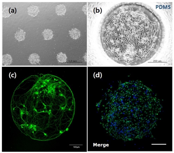
36,54는 가스블로잉 공정으로 PDMS 마이크로스텐실과 마이크로웰 플레이트를 제작하여 신경줄기세포(Neural Stem Cell)와 Purkinje 신경세포 및 인간 골수중간엽 줄기세포의 국부 배양 및 세포분화에 관한 연구를 수행하였다(
Fig. 12). Hsu et al.
55는 신경세포 축삭돌기를 PDMS 스템프와 마이크로스텐실을 이용하여 패턴닝하고 다양한 외인성 단백질(Exogenous Protein) 성장과 시냅스(Synaptic Vesicles)의 분화에 미치는 영향을 연구하였다. Cho et al.
31는 500 μm 크기의 PDMS 스텐실을 이용하여 간세포(Hepatocyte)와 섬유아세포(Fibroblast)를 국부적으로 공동 배양하여 세포의 상호작용을 분석하는 연구를 수행하였다. Chen et al.
56은 PDMS 마이크로스텐실을 다중 채널(Multi-Channel)의 분리를 위한 다공성막(Porous Membrane)으로 사용하여 세포의 공동배양 장치로 응용하였다. Kim et al.
59는 거트 온 어 칩(Gut on a Chip) 모사를 위해 PDMS 마이크로스텐실을 다공성막으로 사용하는 조직공학 연구를 수행하였다. Jinno et al.
57는 Parylene-C 필름을 증착 방법을 통해 제작하고 플라즈마 리엑터(Plasma Reactor)로 식각하여 200 μm 크기의 개방형 패턴을 가지는 다층구조의 Parylene-C 스텐실을 제작하는 방법은 제안하였다. 제작된 스텐실은 단백질과 세포의 공동배양 패터닝으로 활용하였다. Wright et al.
58는 Parylene-C 마이크로스텐실을 제작하여 세포의 공동배양으로 활용하였다.
Fig. 12Bio application : Micropatterned cell culture using PDMS microstencil. (a) and (b) Micropatterned culture of NSCs, (c) Fluorescence image of cortical neurons, (d) Florescence image of NSCs

폴리머 마이크로스텐실의 강한 내구성과 유연성을 이용한 비평면 표면에 구조물 제작 및 패터닝 기술(
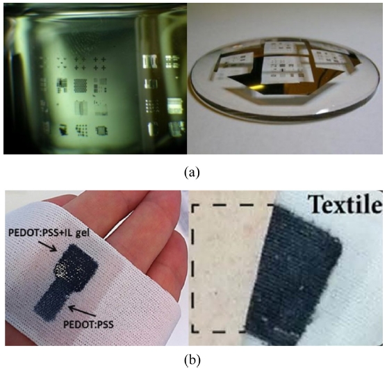
Fig. 13(a))은 플렉시블 디스플레이와 웨어러블 센서의 곡면패터닝 기술과 금속전극 증착 기술로도 연구가 진행되고 있다.
Fig. 13Display application : (a) Aluminum patterns on non-planar surface (Adapted from Ref. 33 with permission), (b) Wearable sensors (Adapted from Ref. 60 on the basis of open access)

Takamatsu et al.
60는 직물(Textile)의 극속 전극 패터닝에 PDMS 스텐실을 사용하여 PEDOT:PSS (Poly 3,4-Ethylenedioxythiophene: Poly Styrene Sulfonate) 전도성 물질을 패터닝 하였으며, 직물에 금속 전극을 제작하여 웨어러블 센서로 활용이 가능한 기술을 보여주었다(
Fig. 13(b)). Meng et al.
61은 PDMS스텐실을 이용한 유연기판에 E-Beam 증착으로 금속 전극을 패터닝하여 변형 센서(Strain Sensor)를 제작하는 연구를 수행하였다. 또한 유연기판에 전도성 물질을 도포하기 위하여 스텐실 리소그래피가 적용되고 있으며 이는 플렉시블 디스플레이로 활용되고 있다.
Yun et al.
62은 전자 빔 리소그래피를 이용하여 PMMA (Polymethylmethacrylate) 기반의 폴리머 스텐실을 제작하여 50 μm에서 500 nm 크기의 다양한 길이를 가지는 전계효과 트랜지스터(Field Effect Transistor, FET) 어레이를 제작하였다.
6. 결론
스텐실 리소그래피 기술의 개발은 확장 가능한 나노/마이크로 제조 분야에서 많은 연구가 진행되었다. 스텐실 리소그래피 기술은 포토레지스트 사용이 없이 대상 기판으로 나노/마이크로 패턴을 전사할 수 있으며, 모재와 증착물질의 선택성이 높고, 고기능 바이오/화학 물질의 표면 패터닝 및 기계적 강성이 약한 구조물의 패터닝이 가능하다. 또한 공정의 간소화, 제조비용의 절감, 재사용 가능 등 나노/마이크로 제조공정에 많은 이점을 제공한다. 이러한 스텐실 리소그래피 기술은 조직공학, 바이오 센싱, 초소형 의료장비, 포토닉스, 플렉시블 디스플레이, 웨어러블 센서 등 다양한 분야로 널리 활용되고 있다.
스텐실은 재료의 성질에 따라 실리콘과 질화실리콘을 기반으로 제작되는 실리콘 기반 스텐실, 금속판을 직접 가공하거나 식각 또는 증착을 통해 제작되는 금속 기반 스텐실, MEMS 공정으로 제작된 마스터 몰드와 폴리머를 이용하여 제작되는 폴리머 기반 스텐실로 분류할 수 있다. 본 논문에서는 스텐실 리소그래피 기술을 개발하기 위한 다양한 연구 그룹의 소개와 제작기법 및 활용성 및 최근 연구 동향을 소개하였다. 실리콘 기반의 스텐실은 실리콘 웨이퍼 상에 증착 된 저응력 SiN 층에 전자 빔 리소그래피와 건식 식각으로 패턴을 정의하고 후면을 KOH로 습식 식각 후 제작되며 패턴 전사 및 금속 나노/마이크로 구조물 제작으로 사용되고 있다. 금속 기반의 스텐실은 금속판을 에첸트를 이용한 습식 식각, 전주도금 방법을 사용한 금속 증착, 레이저를 이용한 금속판의 직접 가공으로 제작되며, OLED 산업과 같은 첨단 디스플레이와 반도체 공정의 식각 및 증착을 위한 마스크로 사용되고 있다. 폴리머 기반 스텐실은 PDMS, 하이드로젤, 광경화성 폴리머 등으로 가압, 흡입, 가스블로잉, 레이져 가공, 펀칭 등의 공정을 사용하여 제작되었다. 이러한 폴리머 기반 스텐실은 신속성, 저비용, 유연성, 생체적합성 등을 가지며 전자산업 및 바이오 공학으로 응용되고 있다.
본 논문에서 소개하는 스텐실 리소그래피 기술은 전통적인 나노 및 마이크로 기술로 제작되는 NEMS 및 MEMS 디바이스 제조 공정의 한계를 극복한 새로운 미세 패터닝 기술이다. 이러한 새로운 미세 패터닝 기술은 조직공학과 바이오 산업을 위한 유용한 도구를 제공할 수 있으며, 첨단 디스플레이 산업의 필수적인 기술로 자리매김 할 것으로 예상된다.
ACKNOWLEDGMENTS
본 논문은 과학기술정보통신부의 재원으로 한국연구재단의 지원을 받아 수행된 연구사업임(NRF-2015R1C1A1A01055210, NRF-2017R1A2B4004966).
REFERENCES
- 1.
Kim, G. and Brugger, J., “Fabrication of Miniaturized Shadow-Mask for Local Deposition,” Journal of Korean Society of Precision Engineering, Vol. 21, No. 8, pp. 152-156, 2004.
- 2.
Chung, S.-I., Oh, H.-S., and Kim, G.-M., “Fabrication of Nanostencil Using FIB Milling for Nanopatterning,” Journal of the Korean Society for Precision Engineering, Vol. 23, No. 3, pp. 56-60, 2006.
- 3.
Kim, C.-K., “The Formation of Micro Metal Patterns Using Shadow Mask,” Proc. of the Korean Society of Manufacturing Technology Engineeres Conference, Vol. 4, pp. 98-99, 2011.
- 4.
Burger, G., Smulders, E., Berenschot, J. W., Lammerink, T. S., Fluitman, J., et al., “High-Resolution Shadow-Mask Patterning in Deep Holes and Its Application to an Electrical Wafer Feed-Through,” Sensors and Actuators A: Physical, Vol. 54, Nos. 1-3, pp. 669-673, 1996.
10.1016/S0924-4247(97)80035-0
- 5.
Ootuka, Y., Ono, K., Shimada, H., and Kobayashi, S.-I., “A New Fabrication Method of Ultra Small Tunnel Junctions,” Physica B: Condensed Matter, Vol. 227, Nos. 1-4, pp. 307-309, 1996.
10.1016/0921-4526(96)00427-9
- 6.
Köhler, J., Albrecht, M., Musil, C., and Bucher, E., “Direct Growth of Nanostructures by Deposition Through an Si3N4 Shadow Mask,” Physica E: Low-Dimensional Systems and Nanostructures, Vol. 4, No. 3, pp. 196-200, 1999.
10.1016/S1386-9477(99)00007-7
- 7.
Deshmukh, M. M., Ralph, D., Thomas, M., and Silcox, J., “Nanofabrication Using a Stencil Mask,” Applied Physics Letters, Vol. 75, No. 11, pp. 1631-1633, 1999.
10.1063/1.124777
- 8.
Brugger, J., Berenschot, J. W., Kuiper, S., Nijdam, W., Otter, B., et al., “Resistless Patterning of Sub-Micron Structures by Evaporation Through Nanostencils,” Microelectronic Engineering, Vol. 53, Nos. 1-4, pp. 403-405, 2000.
10.1016/S0167-9317(00)00343-9
- 9.
Kim, G., Van Den Boogaart, M., and Brugger, J., “Fabrication and Application of a Full Wafer Size Micro/Nanostencil for Multiple Length-Scale Surface Patterning,” Microelectronic Engineering, Vol. 67, pp. 609-614, 2003.
10.1016/S0167-9317(03)00121-7
- 10.
Kim, G.-M., “Focused Ion Beam Milling for Nanostencil Lithography,” Journal of the Korean Society for Precision Engineering, Vol. 28, No. 2, pp. 245-250, 2011.
- 11.
Tun, T. N., Lwin, M. H. T., Kim, H. H., Chandrasekhar, N., and Joachim, C., “Wetting Studies on Au Nanowires Deposited Through Nanostencil Masks,” Nanotechnology, Vol. 18, No. 33, pp. 335301, 2007.
10.1088/0957-4484/18/33/335301
- 12.
Vazquez-Mena, O., Villanueva, G., Savu, V., Sidler, K., Van Den Boogaart, M., et al., “Metallic Nanowires by Full Wafer Stencil Lithography,” Nano Letters, Vol. 8, No. 11, pp. 3675-3682, 2008.
10.1021/nl801778t
- 13.
Kölbel, M., Tjerkstra, R. W., Brugger, J., van Rijn, C. J., Nijdam, W., et al., “Shadow-Mask Evaporation Through Monolayer-Modified Nanostencils,” Nano Letters, Vol. 2, No. 12, pp. 1339-1343, 2002.
10.1021/nl025784o
- 14.
Kölbel, M., Tjerkstra, R. W., Kim, G., Brugger, J., Van Rijn, C. J., et al., “Self Assembled Monolayer Coatings on Nanostencils for the Reduction of Materials Adhesion,” Advanced Functional Materials, Vol. 13, No. 3, pp. 219-224, 2003.
10.1002/adfm.200390033
- 15.
Lee, J. S., Park, W. B., Park, C. W., Hwang, C. S., and Kim, G. M., “Fabrication of Nanostencil by Size Reduction of Microaperture by Additional Deposition,” Japanese Journal of Applied Physics, Vol. 47, No. 6, pp. 5042-5047, 2008.
10.1143/JJAP.47.5042
- 16.
Villanueva, G., Vazquez-Mena, O., Van Den Boogaart, M., Sidler, K., Pataky, K., et al., “Etching of Sub-Micrometer Structures Through Stencil,” Microelectronic Engineering, Vol. 85, Nos. 5-6, pp. 1010-1014, 2008.
10.1016/j.mee.2007.12.068
- 17.
Sidler, K., Villanueva, L. G., Vazquez-Mena, O., Savu, V., and Brugger, J., “Compliant Membranes Improve Resolution in Full-Wafer Micro/Nanostencil Lithography,” Nanoscale, Vol. 4, No. 3, pp. 773-778, 2012.
10.1039/C2NR11609J
- 18.
Özyilmaz, B., Richter, G., Müsgens, N., Fraune, M., Hawraneck, M., et al., “Focused-Ion-Beam Milling Based Nanostencil Mask Fabrication for Spin Transfer Torque Studies,” Journal of Applied Physics, Vol. 101, No. 6, Paper No. 063920, 2007.
10.1063/1.2711785
- 19.
Park, C. W., Mena, O. V., and Brugger, J., “Patterning of Parallel Nanobridge Structures by Reverse Nanostencil Lithography Using an Edge-Patterned Stencil,” Nanotechnology, Vol. 18, No. 4, Paper No. 044002, 2006.
10.1088/0957-4484/18/4/044002
- 20.
Park, C. W., Vazquez Mena, O., Van Den Boogaart, M. A., and Brugger, J., “Reverse Transfer of Nanostencil Patterns Using Intermediate Sacrificial Layer and Lift-Off Process,” Journal of Vacuum Science & Technology B, Vol. 24, No. 6, pp. 2772-2775, 2006.
10.1116/1.2366610
- 21.
Du, K., Ding, J., Wathuthanthri, I., and Choi, C.-H., “Selective Hierarchical Patterning of Silicon Nanostructures Via Soft Nanostencil Lithography,” Nanotechnology, Vol. 28, No. 46, Paper No. 465303, 2017.
10.1088/1361-6528/aa8ce8
- 22.
Agarwal, P. B., Pawar, S., Reddy, S. M., Mishra, P., and Agarwal, A., “Reusable Silicon Shadow Mask with Sub-5 μm Gap for Low Cost Patterning,” Sensors and Actuators A: Physical, Vol. 242, pp. 67-72, 2016.
10.1016/j.sna.2016.02.040
- 23.
Van Den Boogaart, M. A., Lishchynska, M., Doeswijk, L. M., Greer, J. C., and Brugger, J., “Corrugated Membranes for Improved Pattern Definition with Micro/Nanostencil Lithography,” Sensors and Actuators A: Physical, Vol. 130, pp. 568-574, 2006.
10.1016/j.sna.2005.08.037
- 24.
Chung, I.-Y., Kang, K.-H., Kim, J.-D., Sohn, I.-B., Noh, Y.-C., et al., “Femtosecond Pulsed Laser Ablation of OLED Shadow Mask Invar Alloy,” Journal of the Korean Society for Precision Engineering, Vol. 24, No. 12, pp. 50-56, 2007.
- 25.
Jeerapan, I., Sempionatto, J. R., Pavinatto, A., You, J.-M., and Wang, J., “Stretchable Biofuel Cells as Wearable Textile-Based Self-Powered Sensors,” Journal of Materials Chemistry A, Vol. 4, No. 47, pp. 18342-18353, 2016.
10.1039/C6TA08358G
- 26.
Malzahn, K., Windmiller, J. R., Valdés-Ramírez, G., Schöning, M. J., and Wang, J., “Wearable Electrochemical Sensors for in Situ Analysis in Marine Environments,” Analyst, Vol. 136, No. 14, pp. 2912-2917, 2011.
10.1039/c1an15193b
- 27.
Mishra, R. K., Hubble, L. J., Martín, A., Kumar, R., Barfidokht, A., et al., “Wearable Flexible and Stretchable Glove Biosensor for On-Site Detection of Organophosphorus Chemical Threats,” ACS Sensors, Vol. 2, No. 4, pp. 553-561, 2017.
10.1021/acssensors.7b00051
- 28.
Folch, A., Jo, B. H., Hurtado, O., Beebe, D. J., and Toner, M., “Microfabricated Elastomeric Stencils for Micropatterning Cell Cultures,” Journal of Biomedical Materials Research: An Official Journal of The Society for Biomaterials, The Japanese Society for Biomaterials, and The Australian Society for Biomaterials and the Korean Society for Biomaterials, Vol. 52, No. 2, pp. 346-353, 2000.
10.1002/1097-4636(200011)52:2<346::AID-JBM14>3.0.CO;2-H
- 29.
Tourovskaia, A., Barber, T., Wickes, B. T., Hirdes, D., Grin, B., et al., “Micropatterns of Chemisorbed Cell Adhesion-Repellent Films Using Oxygen Plasma Etching and Elastomeric Masks,” Langmuir, Vol. 19, No. 11, pp. 4754-4764, 2003.
10.1021/la0267948
- 30.
Park, J., Cho, C. H., Parashurama, N., Li, Y., Berthiaume, F., et al., “Microfabrication-Based Modulation of Embryonic Stem Cell Differentiation,” Lab on a Chip, Vol. 7, No. 8, pp. 1018-1028, 2007.
10.1039/b704739h
- 31.
Cho, C. H., Park, J., Tilles, A. W., Berthiaume, F., Toner, M., et al., “Layered Patterning of Hepatocytes in Co-Culture Systems Using Microfabricated Stencils,” Biotechniques, Vol. 48, No. 1, pp. 47-52, 2010.
10.2144/000113317
- 32.
Hattori, K., Sugiura, S., and Kanamori, T., “On Chip Cell Culture on a Microarray of Extracellular Matrix with Surface Modification of Poly (Dimethylsiloxane),” Biotechnology Journal, Vol. 5, No. 5, pp. 463-469, 2010.
10.1002/biot.201000021
- 33.
Choi, J. H. and Kim, G. M., “Micro-Patterning on Non-Planar Surface Using Flexible Microstencil,” International Journal of Precision Engineering and Manufacturing, Vol. 12, No. 1, pp. 165-168, 2011.
10.1007/s12541-011-0023-x
- 34.
Li, W., Xu, Z., Huang, J., Lin, X., Luo, R., et al., “Neuroarray: A Universal Interface for Patterning and Interrogating Neural Circuitry with Single Cell Resolution,” Scientific Reports, Vol. 4, No. 4784, pp. 1-7, 2014.
10.1038/srep04784
- 35.
Choi, J. H. and Kim, G. M., “Fabrication of PDMS Stencil Using Gas Blowing for Micropatterned 3T3 Cell Culture,” Journal of the Korean Society for Precision Engineering, Vol. 30, No. 2, pp. 236-240, 2013.
10.7736/KSPE.2013.30.2.236
- 36.
Choi, J. H., Lee, H., Jin, H. K., Bae, J.-S., and Kim, G. M., “Micropatterning of Neural Stem Cells and Purkinje Neurons Using a Polydimethylsiloxane (PDMS) Stencil,” Lab on a Chip, Vol. 12, No. 23, pp. 5045-5050, 2012.
10.1039/c2lc40764g
- 37.
Shiku, H., Takeda, M., Murata, T., Akiba, U., Hamada, F., et al., “Development of Electrochemical Reporter Assay Using Hela Cells Transfected with Vector Plasmids Encoding Various Responsive Elements,” Analytica Chimica Acta, Vol. 640, Nos. 1-2, pp. 87-92, 2009.
10.1016/j.aca.2009.03.018
- 38.
Raof, N. A., Raja, W. K., Castracane, J., and Xie, Y., “Bioengineering Embryonic Stem Cell Microenvironments for Exploring Inhibitory Effects on Metastatic Breast Cancer Cells,” Biomaterials, Vol. 32, No. 17, pp. 4130-4139, 2011.
10.1016/j.biomaterials.2011.02.035
- 39.
Nam, Y., Musick, K., and Wheeler, B. C., “Application of a PDMS Microstencil as a Replaceable Insulator Toward a Single-Use Planar Microelectrode Array,” Biomedical Microdevices, Vol. 8, No. 4, pp. 375-381, 2006.
10.1007/s10544-006-9145-9
- 40.
Choi, J. H. and Kim, G. M., “Development of an Air-Knife System for Highly Reproducible Fabrication of Polydimethylsiloxane Microstencils,” Journal of Micromechanics and Microengineering, Vol. 25, No. 8, Paper No. 085014, 2015.
10.1088/0960-1317/25/8/085014
- 41.
Choi, J. H., Jin, H. K., Bae, J. S., and Kim, G. M., “Fabrication of Three-Dimensional Complex Shape PDMS Microstencil Using Air-Knife System and their Cell Culture Application,” Journal of the Korean Society for Precision Engineering, Vol. 35, No. 1, pp. 111-115, 2018.
10.7736/KSPE.2018.35.1.111
- 42.
Kim, C. M., Lee, H. B., Kim, J. U., and Kim, G. M., “Fabrication of Poly (Lactic-Co-Glycolic Acid) Microcontainers Using Solvent Evaporation with Polydimethylsiloxane Stencil,” Journal of Micromechanics and Microengineering, Vol. 27, No. 12, Paper No. 125018, 2017.
10.1088/1361-6439/aa9591
- 43.
Lee, J., Kim, J. Y., Choi, J. H., Ok, J. G., and Kwak, M. K., “Scalable Fabrication of Flexible Microstencils by Using Sequentially Induced Dewetting Phenomenon,” ACS Omega, Vol. 2, No. 3, pp. 1097-1103, 2017.
10.1021/acsomega.7b00070
- 44.
Khademhosseini, A., Yeh, J., Jon, S., Eng, G., Suh, K. Y., et al., “Molded Polyethylene Glycol Microstructures for Capturing Cells Within Microfluidic Channels,” Lab on a Chip, Vol. 4, No. 5, pp. 425-430, 2004.
10.1039/b404842c
- 45.
Flickinger, S. T., Copeland, M. F., Downes, E. M., Braasch, A. T., Tuson, H. H., et al., “Quorum Sensing Between Pseudomonas Aeruginosa Biofilms Accelerates Cell Growth,” Journal of the American Chemical Society, Vol. 133, No. 15, pp. 5966-5975, 2011.
10.1021/ja111131f
- 46.
Pan, J., Yung Chan, S., Common, J. E., Amini, S., Miserez, A., et al., “Fabrication of a 3D Hair Follicle Like Hydrogel by Soft Lithography,” Journal of Biomedical Materials Research Part A, Vol. 101, No. 11, pp. 3159-3169, 2013.
10.1002/jbm.a.34628
- 47.
Choi, J. H., Kim, Y. H., Choi, S. D., and Kim, G. M., “Preparation of 3D Electrode Microarrays of Multi-Walled Carbon Nanotubes/Nafion Nanocomposites for Microfluidic Biofuel Cells,” Journal of Nanoscience and Nanotechnology, Vol. 14, No. 12, pp. 9323-9328, 2014.
10.1166/jnn.2014.10116
- 48.
Choi, S. D., Choi, J. H., Kim, Y. H., Kim, S. Y., Dwivedi, P. K., et al., “Enzyme Immobilization on Microelectrode Arrays of CNT/Nafion Nanocomposites Fabricated Using Hydrogel Microstencils,” Microelectronic Engineering, Vol. 141, No. pp. 193-197, 2015.
10.1016/j.mee.2015.03.045
- 49.
Fukuda, J., Khademhosseini, A., Yeo, Y., Yang, X., Yeh, J., et al., “Micromolding of Photocrosslinkable Chitosan Hydrogel for Spheroid Microarray and Co-Cultures,” Biomaterials, Vol. 27, No. 30, pp. 5259-5267, 2006.
10.1016/j.biomaterials.2006.05.044
- 50.
Masters, T., Engl, W., Weng, Z. L., Arasi, B., Gauthier, N., et al., “Easy Fabrication of Thin Membranes with Through Holes. Application to Protein Patterning,” PLoS One, Vol. 7, No. 8, Paper No. 0044261, 2012.
10.1371/journal.pone.0044261
- 51.
Rana, K., Timmer, B. J., and Neeves, K. B., “A Combined Microfluidic-Microstencil Method for Patterning Biomolecules and Cells,” Biomicrofluidics, Vol. 8, No. 5, pp. 1-10, 2014.
10.1063/1.4896231
- 52.
Shimizu, K., Fujita, H., and Nagamori, E., “Micropatterning of Single Myotubes on a Thermoresponsive Culture Surface Using Elastic Stencil Membranes for Single-Cell Analysis,” Journal of Bioscience and Bioengineering, Vol. 109, No. 2, pp. 174-178, 2010.
10.1016/j.jbiosc.2009.07.016
- 53.
Wu, H.-I., Cheng, G.-H., Wong, Y.-Y., Lin, C.-M., Fang, W., et al., “A Lab-on-a-Chip Platform for Studying the Subcellular Functional Proteome of Neuronal Axons,” Lab on a Chip, Vol. 10, No. 5, pp. 647-653, 2010.
10.1039/B918217A
- 54.
Choi, J. H., Bae, J.-S., Lee, H., Jin, H. K., and Kim, G. M., “Micropatterned Culture and Differentiation of Human Bone Marrow Mesenchymal Stem Cells Using a Polydimethylsiloxane Microstencil,” Journal of Biomedical Nanotechnology, Vol. 12, No. 2, pp. 366-370, 2016.
10.1166/jbn.2016.2186
- 55.
Hsu, Y.-H., Wu, H.-I., Cheng, W.-S., Chung, H.-W., Wu, T.-Y., et al., “A Chip-Based Method for Studying the Effects of Exogenous Proteins on Neuronal Axons,” Analytical Biochemistry, Vol. 427, No. 1, pp. 1-9, 2012.
10.1016/j.ab.2012.04.017
- 56.
Chen, L.-J., Ito, S., Kai, H., Nagamine, K., Nagai, N., et al., “Microfluidic Co-Cultures of Retinal Pigment Epithelial Cells and Vascular Endothelial Cells to Investigate Choroidal Angiogenesis,” Scientific Reports, Vol. 7, No. 1, Paper No. 3538, 2017.
10.1038/s41598-017-03788-5
- 57.
Jinno, S., Moeller, H. C., Chen, C. L., Rajalingam, B., Chung, B. G., et al., “Microfabricated Multilayer Parylene C Stencils for the Generation of Patterned Dynamic Co Cultures,” Journal of Biomedical Materials Research Part A, Vol. 86, No. 1, pp. 278-288, 2008.
10.1002/jbm.a.32030
- 58.
Wright, D., Rajalingam, B., Selvarasah, S., Dokmeci, M. R., et al., “Generation of Static and Dynamic Patterned Co-Cultures Using Microfabricated Parylene-C Stencils,” Lab on a Chip, Vol. 7, No. 10, pp. 1272-1279, 2007.
10.1039/b706081e
- 59.
Kim, H. J., Huh, D., Hamilton, G., and Ingber, D. E., “Human Gut-on-a-Chip Inhabited by Microbial Flora that Experiences Intestinal Peristalsis-Like Motions and Flow,” Lab on a Chip, Vol. 12, No. 12, pp. 2165-2174, 2012.
10.1039/c2lc40074j
- 60.
Takamatsu, S., Lonjaret, T., Crisp, D., Badier, J.-M., Malliaras, G. G., et al., “Direct Patterning of Organic Conductors on Knitted Textiles for Long-Term Electrocardiography,” Scientific Reports, Vol. 5, pp. 15003, 2015.
10.1038/srep15003
- 61.
Meng, L., Mahpeykar, S. M., Xiong, Q., Ahvazi, B., and Wang, X., “Strain Sensors on Water-Soluble Cellulose Nanofibril Paper by Polydimethylsiloxane (PDMS) Stencil Lithography,” RSC Advances, Vol. 6, No. 88, pp. 85427-85433, 2016.
10.1039/C6RA10069D
- 62.
Yun, H., Kim, S., Kim, H., Lee, J., McAllister, K., et al., “Stencil Nano Lithography Based on a Nanoscale Polymer Shadow Mask: Towards Organic Nanoelectronics,” Scientific Reports, Vol. 5, pp. 1-8, 2015.
10.1038/srep10220
Biography
- Jin Ho Choi
Ph.D./Researcher in the Institute of Mechanical Engineering Technology, Kyungpook National University. His research interest is Micro-Electro Mechanical System.
- Hye Jin Choi
Ph.D. candidate in the School of Mechanical Engineering, Kyungpook National University. Her research interest is Micro-Electro Mechanical System.
- Gyu Man Kim
Professor in the School of Mechanical Engineering, Kyungpook National University. His research interest is Micro-Electro Mechanical System.