ABSTRACT
Chemical mechanical planarization (CMP) is a semiconductor process which is necessary for multi-layer interconnection structure. CMP pad is a consumable used in the process and with numerous asperities on the surface that wear out by the load applied from the contact with the wafer. Also, it has a patterned wafer, the step height is gradually removed by contact of the asperities with upper and lower layers. The contact state would be different according to the step height reduction. Likewise, depending on the pattern size at the specific step height, the maximum radius of the asperity curvature differs whether it reaches the down area. In this study, the height distribution of asperities was expressed as a function of time and asperity height taking into account the wear of asperities, and based on the Greenwood-Williamson theory, a mathematical model for material removal rate considering pattern size was derived. The consistency of the novel model is verified with the CMP experiment conducted using oxide patterned wafers, and the experimental data were compared with the residual step height using theoretical removal rate. The root mean square error of the step height reduction was 19.84 nm.
-
KEYWORDS: Chemical mechanical planarization, Mathematical modeling, Pad asperity, Distribution of asperity height, Pattern size
-
KEYWORDS: 화학 기계적 평탄화 공정, 수학적 모델링, 패드 돌기, 돌기 높이 분포, 패턴 크기
NOMENCLATURE
Contact area in up or down area
Nominal area in whole wafer
Contact area in blanket wafer
Wear coefficient of pad asperity
Effective height of pad asperity
Contact height of pad asperity
Contact load on up or down area
Nominal load on whole wafer
Contact load on blanket wafer
Material removal rate by single asperity
Material removal rate for patterned wafer
Material removal rate for blanket wafer
Material removal rate for up or down area
Material removal rate for blanket wafer
Contacted number of pad asperity
Contacted number of pad asperity in up or down area
Contacted number of pad asperity in blanket wafer
Total number of pad asperity
Contact pressure on single asperity
Contact pressure on up and down area
Radius of pad asperity curvature
Max asperity radius contactable to down area
Width of space in pattern
Substitution index for pad wear
Distance from contact interface to pad reference plane
Shape parameter of contacted asperity with pattern
Fraction of contactable asperities to down area
Effective pad asperity curvature
Pad asperity curvature on up or down area
Substitution index for effective pattern density
Mean radius of pad asperity curvature
Effective pattern density
Deviation of distribution of pad asperity height
Deviation of distribution of pad asperity radius
Substitution index in expression of contact area
Substitution index in expression of contact load
Distribution of pad asperity height
Distribution of pad asperity radius
Substitution index for time dependent distribution of pad asperity height
1. 서론
화학 기계적 연마 또는 화학 기계적 평탄화(Chemical Mechanical Polishing/Planarization, CMP) 공정은 소자의 고집적화 및 다층배선구조를 형성하기 위해 디바이스화 공정에서 발생하는 표면의 요철을 연마하여 박막을 평탄화시키기 위해 필요한 반도체 공정이다.
1 CMP 공정은 화학적 작용과 기계적 작용을 결합한 평탄화 기술로
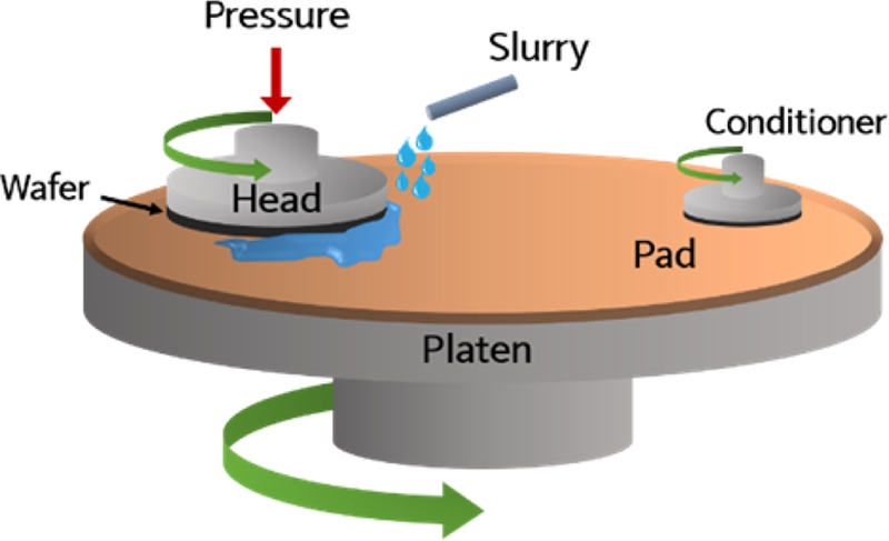
Fig. 1과 같이 웨이퍼와 CMP 패드 간의 상대 회전에 의한 물리적 마찰과 슬러리(Slurry)의 화학 반응에 의한 마멸이 발생함으로써 연마가 진행된다.
2
Fig. 1 Schematic of a typical single-wafer CMP tool

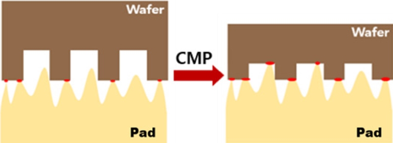
이상적인 패턴 웨이퍼에 대한 CMP 메커니즘은 요철의 상부 영역에서만 연마가 일어나 단차가 점진적으로 제거되는 것으로, 국부적으로 단차가 사라지기 전까지 하부에서의 연마는 진행되지 않는다고 가정한다.
2 그러나 Lee. B
3의 단차 밀도 모델(Step Height Density Model)에서는 실제 패턴 CMP 경우
Fig. 2와 같이 단차가 큰 연마 초기 단계에서는 하부의 연마가 진행되지 않으나, 단차의 감소로 특정 높이에 도달한 이후에는 상하부 층에서 동시에 연마가 일어나며, 이를 접촉 높이(Contact Height)라고 정의하였다. 한편 접촉 높이, 즉 하부 연마가 시작되는 단차는 패턴의 밀도 및 크기와 같은 기하학적 형상에 따라 달라진다. 이로 인해 다양한 패턴이 설계된 디바이스 패턴을 가공할 경우 단차 제거 속도의 차이로 인해 하나의 다이(Die)내에서도 국부적으로 연마 불균일이 초래된다.
4 이러한 연마 불균일이 발생하는데에 있어서 하부 연마에 대해 패턴의 형상뿐만 아니라 패드 돌기의 특성이 미치는 영향이 크게 기인한다.
5 폴리우레탄 재질의 연마 패드에는 불규칙적인 높이와 직경을 가진 돌기들이 분포되어 있고 공정 시 돌기와 웨이퍼 간의 접촉에 의해 연마가 진행된다. 이러한 공정 중 접촉에 의해 패드 돌기는 연마에 참여하는 동시에 마모가 진행되는데, 이는 돌기 높이 분포를 변화시킴으로써 표면 거칠기를 감소시키는 원인이 되며, 이에 따라 연마율이 감소하는 결과를 초래한다.
6 따라서 디바이스 패턴에 대한 연마 경향을 보다 정확히 예측하기 위해서는 패턴의 형상 및 패드 돌기의 기하학적 및 기계적 특성을 함께 고려하여 접촉 메커니즘을 정의하여 이를 기반으로 평탄화 모델을 도출하는 것이 바람직하다.
Fig. 2 Step height density model
Tang. B
7는 디바이스 패턴에서 인접해있는 패턴의 형상이 미치는 영향을 고려하여 유효 패턴 밀도(Effective Pattern Density)를 적용하고 패턴 하부의 연마가 시작되는 시점을 기준점으로 CMP 메커니즘을 나누어 도출한 평탄화 모델을 제시하였다. Vasilev. B
8는 Greenwood-Williamson (GW) 접촉 이론을 기반으로 패턴 웨이퍼에서 접촉 계면에서의 유효 돌기 곡률(Effective Asperity Curvature) 및 패턴 밀도를 고려하여 패턴 CMP에 적용할 수 있도록 물리적 모델을 도출하였다. Kim. H
9는 산화막 패턴에 대하여 패드 돌기의 변형 특성을 고려하여 접촉 모드에 따라 Ref. 8의 물리적 모델을 세분화하여 최종적으로 재료제거율 식을 제시하였다. 언급한 디바이스 패턴의 평탄화 모델과 관련된 선행 연구의 경우 패턴 밀도를 고려하여 상하부에 따른 연마율을 세분화하여 제시하였으나 돌기의 지형학적 특성이 미치는 영향은 배제되어 있거나, 패턴 밀도 및 패드 돌기의 기계적 특성을 고려하여 패턴의 상하부 및 돌기의 변형에 따라 접촉 모드를 세분화하여 제시하였으나 공정 시간에 따라 변화하는 돌기 높이 분포의 변화에 대응할 수 없다는 한계점이 존재하며 패턴 하부 영역의 너비가 패드 돌기의 직경보다 좁은 미세 패턴에서의 접촉 메커니즘에 대한 연구가 필요하다.
본 연구에서는 시간에 따른 돌기 높이 분포의 변화를 표현하는 확률 밀도 함수(Probability Density Function, PDF)를 정의하여 GW 접촉 모델에 적용하고 패턴과 패드 돌기의 기하학적 상관 관계가 미치는 영향을 고려하여 수학적 모델링을 진행하였다.
2. 이론적 배경
2.1 Greenwood-Williamson 접촉
Greenwood와 Williamson
10은
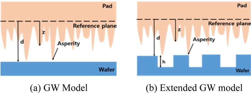
Fig. 3(a)와 같이 크기와 높이가 불규칙적인 돌기가 분포된 표면 형상에 대하여 무작위의 돌기 높이를 지수분포로 표현하여 접촉 이론을 제시하였다.
Fig. 3GW contact theory

여기서
σ는 돌기 높이 분포의 편차이며
z는 돌기 높이를 의미한다. 지수 함수로 표현되는 돌기 높이 분포를 기반으로 접촉에 의한 돌기의 변형량을 계산하기 위해서는 참조면으로부터 접촉 계면까지의 거리를 설정해야 하므로 이러한 가상의 거리를 유효 돌기 높이
d로 정의하였다. 따라서 불규칙한 표면에서 단일 돌기에 대한 접촉 하중, 접촉 면적 그리고 확률적 접근에 근거한 접촉 돌기 개수를 다음
식(2)부터
식(4)와 같이 표현할 수 있다.
E*는 E* = E/(1 - v2)으로 E는 패드의 탄성 계수, v는 프와송 비이다. 또 κ는 돌기의 곡률, N은 전체 돌기의 개수를 의미한다. 기존의 GW 모델의 경우 박막 웨이퍼에 대한 접촉 이론으로 패턴 웨이퍼에 대해 적용하기 위해서는 패턴 형상이 기하학적으로 주는 영향을 고려해야한다.
Vasilev. B는 GW 접촉 이론을 기반으로 단차가 존재하는 산화막 패턴층에 대한 물리적 모델을 패턴의 상·하부 영역에 대해 세분화하여 재료제거율을 도출하였다. 이때 패턴과 패드 돌기의 접촉에 대해 고려할 경우 패턴 상하부에 따라 달라지는 돌기 곡률을 적용시켜야하므로 유효 돌기 곡률(Effective Asperity Curvature) 개념을 도입하였다.
Fig. 4와 같이 유효 돌기 곡률은 기하학적 형상을 고려하여 돌기 곡률을 표현한 것으로 단차와 패턴 크기를 기반으로 다음
식(5)와
식(6)과 같이 표현할 수 있다.
Fig. 4Effective asperity curvature

식(5)과
식(6)에 따르면 패턴 상부 영역과 접촉 시 곡률이 증가하고 하부 영역과 접촉 시 곡률이 감소하게 된다.
기존의 접촉 모델을 패턴의 상하부 층에 따라 세분화하여 패턴 밀도와 각 층에 대한 돌기 곡률을 고려하여
식(7)부터
식(12)와 같이 정리할 수 있다.
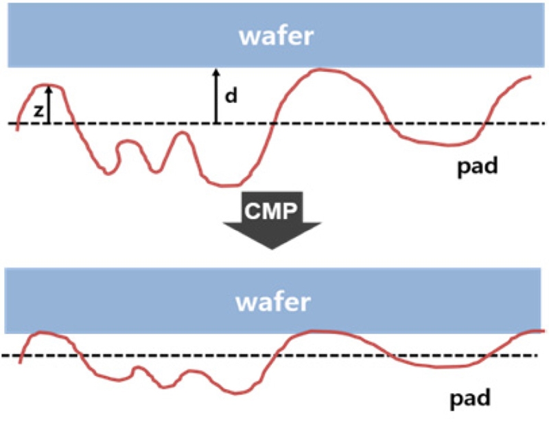
연마 패드는 연마기의 정반(Platen)에 부착하여 사용하며 공정 시 웨이퍼가 부착된 연마 헤드(Head)가 내려와 연마가 진행된다.
11 이때 접촉에 의해 헤드로부터 인가되는 하중을 받아 폴리우레탄 재질의 연마 패드의 미세 돌기는 마모가 발생한다.
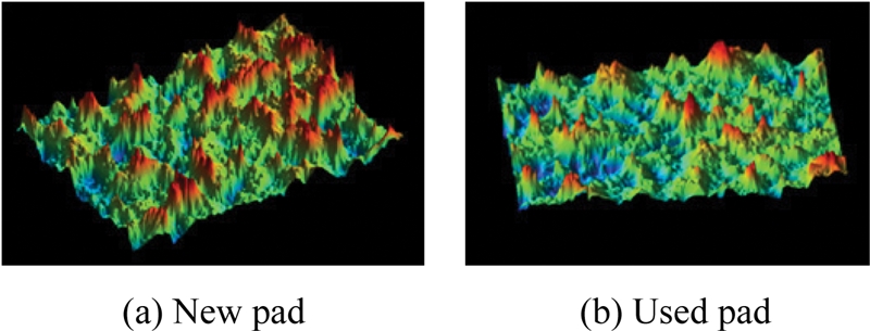
Fig. 5는 공초점 현미경으로 새 패드와 오랫동안 사용하여 마모가 발생한 패드의 표면을 촬영하여 비교한 것으로, 이와 같이 시간이 지남에 따라 계속되는 마모로 인해 패드의 표면 거칠기는 변화하여 안정적으로 연마율을 유지하기 어렵고 초기 연마율에 비해 점차 감소하여 결과적으로 공정의 안정성을 저하시키는 원인이 된다. 돌기의 마모율은 Archard의 법칙에 따라 다음
식(13)과 같이 표현할 수 있다.
12
Fig. 5Pad roughness evolution due to wear of pad asperities
여기서
ca는 웨이퍼에 대한 돌기의 미끄럼 속도에 대한 매개변수이다. Borucki L.
13은 공정 중 패드 돌기의 마모율을 고려하여 돌기 높이 분포를 다음
식(14)와 같이 편미분 방정식의 형태로 표현하였다.
돌기 마모율을 고려한 돌기 높이 분포의 변화를 고려하여 GW 접촉 이론을 기반으로 최종적으로 재료제거율에 대한 식을 얻기 위해서는 돌기 높이 분포에 대한 확률 밀도 함수가 필요하다. 따라서 편미분 형태의
식(14)를 활용하여 수학적으로 도출하는 과정이 필요하며, 이에 대한 자세한 내용은 3.1장에서 다루었다.
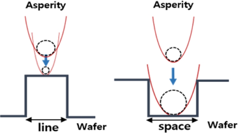
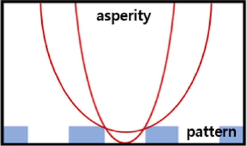
1장에서 언급한 바와 같이 디바이스 패턴에 대한 CMP의 경우 연마에 의해 특정 단차에 도달한 시점부터 상부와 하부 영역에 대한 연마가 동시에 진행된다. 하부 영역에 대한 패드 돌기의 접촉의 경우 돌기 높이의 영향뿐만 아니라 돌기의 곡률 반경 또한 고려해야할 요소이다.
Fig. 6에 돌기 곡률 반경에 따른 돌기와 패턴 간의 접촉 상태를 단순하게 표현하였다. 동일한 단차에 대하여 돌기와 패턴 하부의 접촉을 비교할 경우, 돌기 반경이 감소할수록 하부에 대한 접촉이 쉽게 일어난다. 즉, 트렌치(Trench) 너비보다 큰 돌기의 경우 하부 영역에 도달하기 어려우며 이를 다시 해석하자면 돌기 곡률 반경의 분포에 따라 패턴 하부에 대한 연마에 참여할 수 있는 돌기의 비율이 달라진다. Vasilev B.
14는 패드 거칠기 측정을 통해 돌기의 곡률 반경에 대해 로그 정규분포와 근접하다고 제시하였다. 로그 정규분포 함수를 사용하여 돌기 곡률 반경의 분포를 나타내면 다음
식 (15)와 같다.
Fig. 6Difference of contact state according to asperity radius
따라서, 돌기 곡률 반경의 분포 편차가
σasp이고 로그 정규분포를 따를때, 패턴 하부층에 도달할 수 있는 돌기의 비율은 다음
식(16)과 같이 적분식으로 표현할 수 있다.
여기서 Rmax는 특정 패턴 크기에 대하여 하부층에 도달할 수 있는 돌기의 최대 곡률 반경을 의미한다.
3. 수학적 모델링
본 연구에서는 패턴과 돌기의 접촉 메커니즘에 대한 정의를 위해 GW 접촉 모델과 유효 돌기 곡률 개념을 기반으로 패턴 사이즈와 돌기 반경의 상관관계 및 CMP 가공 시간에 따른 패드 돌기의 마모에 의한 돌기 높이 분포 변화를 고려하여 접촉 모델을
식(17)부터
식(22)와 같이 새롭게 정의하였고 이를 통해 재료제거율에 대한 수학적 모델을 도출하였다.
기존의 GW 접촉 모델의 경우 돌기의 높이 분포를 지수함수로 표현하였다. 그러나 2.2장에서 언급하였듯이 공정 중에는 패드 돌기의 마모가 발생하여 연마 패드의 표면 거칠기가 감소하게 된다.
Fig. 7은 공정 중 웨이퍼와 패드의 접촉에서 마모에 의한 돌기 높이의 변화를 표현한 모식도이다. 패드의 표면 거칠기의 감소가 연마율에 미치는 영향을 고려하기 위해서 돌기 높이 분포에 대하여 돌기의 마모율을 고려하여 시간에 대한 함수로 표현하는 것이 바람직하다.
Fig. 7The evolution of asperity height distribution during CMP
2.2장에서 언급한 돌기 마모에 따른 돌기 높이 분포의 변화에 대한 편미분 방정식을 정리하면 다음
식(24)와 같다.
식(17)부터
식(22)와 같이 새롭게 정의한 물리적 모델을 풀기 위해서는 돌기 높이 분포에 대하여 수학적으로 정의하는 것이 필요하다. 편미분 형태의 식을 풀기 위해 새로운 변수
x를 사용하여
z와
t를
x에 대한 함수로 표현하였고,
z와
t가
x에 대한 함수일 경우
ϕ 또한
식(25)와 같이
x에 대한 함수로 표현할 수 있다.
식(26)부터
식(28)과 같이 세 개의 상미분방정식으로 표현할 수 있다.
식(26)부터
식(28)을 풀기 위해 초기값을 사용한다. 이때
ϕ(
x) =
ϕ0(
z0)로
t = 0일 때, 즉 마모가 발생하기 전 돌기 높이 분포로 기존의 GW 접촉 이론과 같이 사용한 지수함수 형태로 가정하였다.
식(28)을 풀면
x =
t이며
식(27)를 풀면
z0을 다음
식(29)와
식(30)과 같이 표현할 수 있다. 계산에 불필요한 돌기의 마모율 식과 관련된 매개변수들을
w로 치환하여 표현하였다.
단,
식(31)의 경우 돌기 높이가
d보다 클 경우, 즉 돌기와 박막의 접촉이 발생하였을 때에 해당되며,
d보다 작을 경우 접촉이 일어나지 않기 때문에 마모에 의한 돌기 높이 분포의 변화 역시 발생하지 않으므로 초기 분포를 그대로 유지하게 된다.
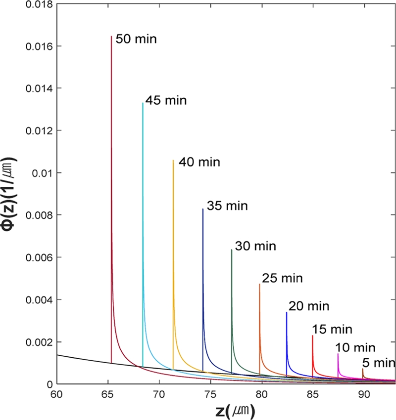
Fig. 8은
식(31)을 사용하여 MATLAB을 통해 시간에 따른 돌기 높이 분포의 변화를 그래프로 나타낸 것으로 가장 아래에 있는 선은 돌기 높이에 대한 초기 분포를 나타낸다. 또한 각 공정 시간에 대한 분포 그래프마다 수직선이 나타나는데 이는
z =
d로 특이점이 나타나는 구간이다. 다시 말하자면
z =
d를 기준점으로
z ≤
d일 경우 초기 분포를 따르고
z >
d일 때 분포의 변화가 발생하므로 시간에 대한 함수로 표현한 식을 따르게 된다.
Fig. 8Simulation of time-dependent asperity height distribution
3.2 유효 돌기 높이(d(t))
일반적으로 CMP의 경우 일정한 압력 하에 진행된다. 가상의 참조면과 웨이퍼의 거리를 의미하는 유효 돌기 높이 d의 경우 하중의 균형을 유지하기 위해서는 돌기 높이 분포의 변화에 따라 유효 돌기 높이 또한 변하므로 d 역시 시간에 대한 함수로 표현하는 것이 바람직하다.
식(17)부터
식(22)에 존재하는 적분항을 정리하기 위해서는 유효 돌기 높이
d(
t)를 알아야한다. 그러나 유효 돌기 높이는 측정을 통해 얻을 수 없으므로 수학적으로 도출해야 한다. 한편, 패턴 웨이퍼와 패드 간의 접촉 시 패턴의 상부층에 대한 접촉 하중과 하부층에 대한 접촉 하중의 합은 연마기의 헤드를 통해 웨이퍼로 인가되는 하중과 동일하므로 힘의 평형방정식을 적용할 수 있으므로
식(33)과 같이 표현할 수 있다.
2장에서 정의한 접촉 하중에 대한
식(17)과
식(18)을
식(33)에 적용하고 3.1장에서 도출한 돌기 높이 분포에 대한
식(31)을 사용하여 적분항을 정리하면
d(
t)에 대한 식을 도출할 수 있다.
식(35)부터
식(38)에서
ψt, λU, λD,τLU,Dt은 식을 간단하게 정리하기 위해 사용한 치환계수이다.
2.3장에서 언급하였듯이 패턴 하부 영역에 대한 패드 돌기의 접촉의 경우 돌기의 곡률 반경은 중요하게 작용한다. 돌기에 비해 큰 패턴의 경우 돌기의 크기가 주는 영향은 미미하나, 미세 패턴의 경우 하부의 너비의 한계로 하부에 접촉할 수 있는 돌기가 줄어들게 되면서 하부 연마에 큰 영향을 미치게 된다.
Fig. 9와 같이 단차가 같고 서로 다른 피치를 가지는 패턴과 단일 돌기의 접촉 상태에 대한 모식도이다. 트렌치의 너비가 좁아질수록 하부에 대한 돌기의 통과는 어려워지며 하부 영역에 접촉하지 못하는 돌기는 상부 연마에 참여하게 되므로 결과적으로 트렌치의 너비가 좁아질수록 상부의 연마량이 증가할 것임을 예측할 수 있다.
Fig. 10과 같은 패턴에서 주어진 패턴 크기에 대해 하부 영역에 접촉할 수 있는 최대 돌기 반경을
Rmax, 이때의 단차를
hc라고 정의하였다. 하부층의 너비를
s라 할 때,
Rmax,
hc 그리고
s의 관계를 다음
식(39)와 같이 표현할 수 있다.
Fig. 9The contact state between trench and single asperity
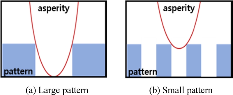
Fig. 10Schematics of the max asperity radius contactable to the down area
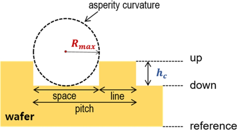
식(39)를 정리하면
식(40)과 같이 특정 크기의 패턴에 대하여 하부 영역에 접촉할 수 있는 돌기 반경의 최댓값을 표현할 수 있다.
식(40)을 통해서 얻은
Rmax의 경우
식(16)에 존재하는 적분에 대하여 적분 상한으로 사용할 수 있다. 즉, 하부의 너비가
s인 패턴의 단차가
hc일 때 해당 패턴의 하부에 접촉할 수 있는 돌기의 최대 반경을 설정하여 전체 돌기 반경 분포에 대하여 실제로 하부 연마에 참여할 수 있는 돌기의 비율을 예측할 수 있다.
3.4 GW 접촉 이론 기반의 새로운 모델
3.4.1 접촉에 대한 물리적 모델
2.1장에서 언급한 GW 접촉 이론을 기반으로 하여 가공 시간에 따른 패드 돌기의 높이 분포 변화 및 패턴의 크기와 돌기 반경의 상관관계를 고려하여 접촉 하중, 접촉 면적 그리고 접촉 돌기 개수에 대한 식을 새롭게 정의하여 적분항을 풀면
식(41)부터
식(46)과 같이 웨이퍼에 인가되는 하중(
LW)에 대한 함수로 정리할 수 있다. 접촉 면적 식에 대해 보다 간단한 식 정리를 위해
식(47)과 같이 치환계수를 사용하였다.
3.4.2 재료제거율
일반적으로 재료제거율에 대한 식은 지배방정식으로 프레스톤 식을 사용한다.
15
여기서
kp는 프레스톤 상수,
P는 공칭 압력,
V는 웨이퍼와 패드 간의 상대 회전속도를 의미한다.
식(48)은 웨이퍼 전면에 대한 재료제거율로, 단차가 존재하는 패턴 웨이퍼를 대상으로 할 경우 상부 및 하부 영역을 따로 정의하는 것이 필요하다. 따라서 상하부 영역에 대한 재료제거율 식을 얻기 위해 3.4.1장에서 제시한 모델 식으로부터 정의된 매개변수를 사용한다. 패턴의 경우 상하부에 따라 접촉하는 돌기의 개수가 달라지므로 이를 고려하기 위해서는 단일 돌기에 대한 재료제거율 식이 필요하다.
여기서
Pasp는 단일 돌기에 대한 압력으로
Pasp =
Lasp/
Aasp이므로 단일 돌기에 대한 접촉 하중을 접촉 면적으로 나눈 값으로 정의된다.
식(49)를 사용하여 웨이퍼에 대한 재료제거율에 대한
식(48)은
식(50)과 같이 표현할 수 있다. 여기서
AW는 웨이퍼 전면의 면적을 의미한다.
식(54)를 다시 정리하면
식(55)와 같이
kp와
kp'의 관계를 나타내는 식으로 표현할 수 있다.
한편, 패턴 웨이퍼에 대한 재료제거율의 경우 패턴 상부 영역과 하부 영역에 대하여 나누어 정의하는 것이 필요하다. 각 영역에 대한 재료제거율 식을 표현하기 위해서는 유효 패턴 밀도(ρeff)와 유효 돌기 곡률(κ)의 개념을 적용하여 패턴의 기하학적 특성이 연마 결과에 미치는 영향을 고려할 수 있도록 한다.
식(56)에서
PaspU,D 및 nU,D은 각각 패턴의 상하부 영역에 대한 단일 돌기의 접촉 압력과 접촉 돌기 개수를 의미한다.
PaspU,D의 경우 3.4.1장에서 얻은 접촉 하중, 접촉 면적에 대한 식을 접촉하는 돌기의 개수에 대한 식으로 나눈 값과 같으므로 다음
식(57)과 같이 표현할 수 있다.
식(56)에 대하여 단차가 0이 되었을 때 재료제거율은 다음
식(58)과 같이 표현할 수 있다.
또한 시간 t0에서부터 t1 동안의 박막의 총 제거량은 재료제거율 MRR(t)을 해당 시간 동안에 걸쳐 적분을 함으로써 얻을 수 있다.
4. 실험 및 모델 검증
4.1 실험 조건
본 연구에서 제시한 모델에 대하여 실제 공정 조건 하에 시뮬레이션에 대한 결과가 실제 공정 결과와 얼마나 유사한지 정합성을 분석하기 위해 CMP 실험을 진행하였다. 실험은
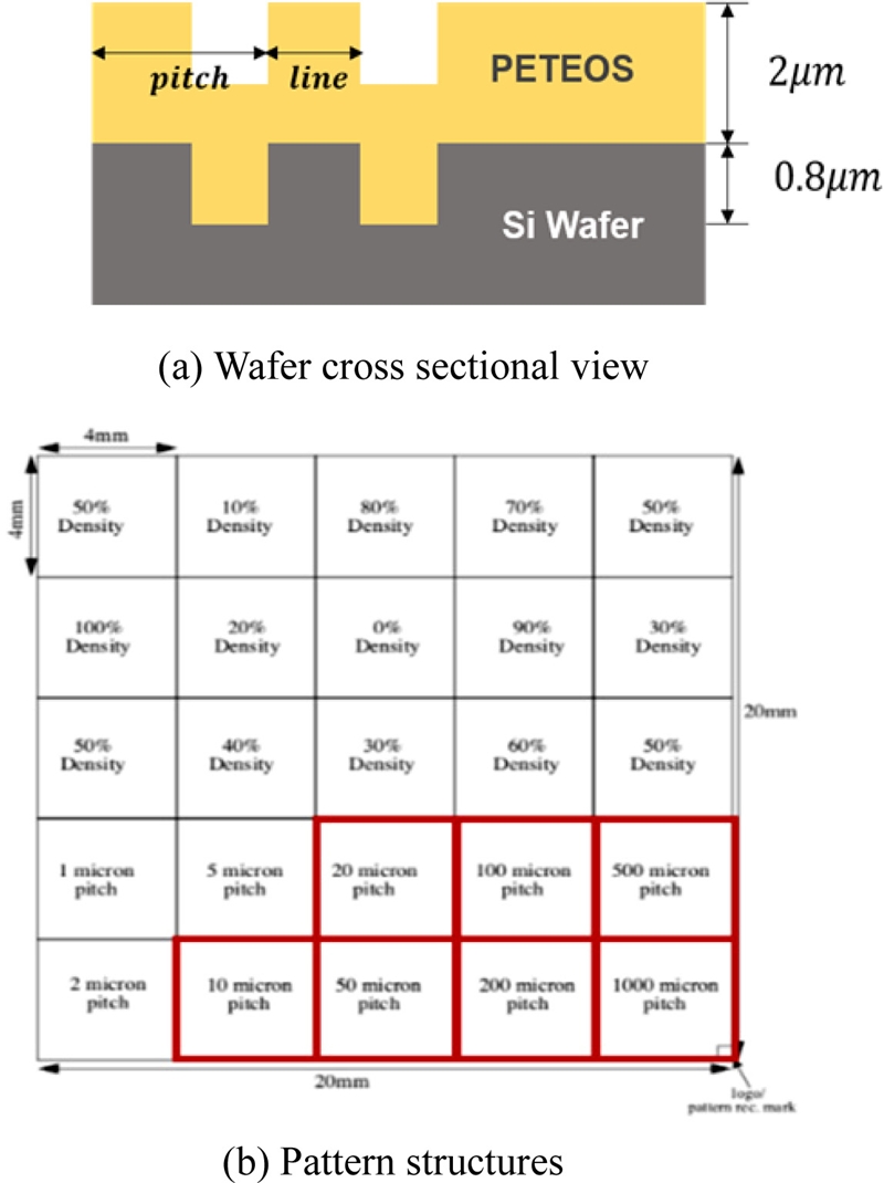
Fig. 11(a)와 같은 단면 구조로 패터닝된 200 mm의 산화막 패턴 웨이퍼를 대상으로 하였고 G&P Technology사의 POLI-500을 사용하여 CMP를 하였다.
Fig. 11(b)에서는 패턴 배치 정보를 확인할 수 있으며 모델 검증의 경우 10에서 100 μm까지 패턴의 피치가 변화하는 영역을 대상으로 하였다. 연마의 경우 1분부터 5분까지 각 웨이퍼당 1분 간격으로 연마 시간을 증가시키면서 진행하였다. 그 외 CMP 공정 시 사용한 소모품 및 공정 조건의 경우
Table 1에 제시하였다. 연마를 시작하기에 앞서 연마 패드의 안정화를 위해 20분간 Break-In 공정을 실시하였고 공정이 한 번 끝날 때마다 컨디셔닝 공정을 5분간 진행하였다.
Fig. 11Information of device pattern for the experiment

Table 1Experimental conditions
Table 1
|
Target |
200 mm patterned wafers
coated with PETEOS |
|
Pad |
IC1000 |
|
Slurry |
Fumed silica |
Pressure
[psi] |
Head |
2 |
|
Retainer |
3 |
Velocity
[rpm] |
Head |
93 |
|
Platen |
87 |
|
Slurry flow rate [ml/min] |
150 |
|
Conditioning |
Ex-situ |
4.2 실험 결과 및 모델 검증
CMP 후 잔여 산화막 두께를 KMAC사의 박막 두께 측정기를 사용하여 측정하였다. 패턴의 피치에 따른 잔여 단차를 비교하기 위해 패턴의 상부 및 하부 영역에 대한 잔여 박막 두께를 측정한 뒤 단차를 계산하였다. 이러한 실제 공정 데이터를 MATLAB에서 시뮬레이션을 통해 얻은 결과와 비교 분석하였다. 시뮬레이션을 위해 사용한 물성의 경우
Table 2에 제시되어 있으며 NANOSCOPE사의 공초점 현미경을 사용하여 돌기의 평균 곡률 반경을 측정하였으며 그 외의 패드 물성의 경우 Refs. 16, 17의 IC1000에 대한 물성 데이터를 참고하였다.
16,17
Table 2Mechanical properties of CMP pad
Table 2
|
Pad modulus (E*) [GPa] |
2.2 |
|
Wear coefficient (ca) [m/sec/Pa] |
2.5×10⁻¹⁶
|
|
Mean radius of asperity (μ) [μm] |
23.5 |
|
Mean asperity curvature (κ) [μm-1] |
0.0426 |
|
Deviation of asperity height (σ) [μm] |
4.4 |
|
Deviation of asperity radius (σasp) [μm] |
10.7 |
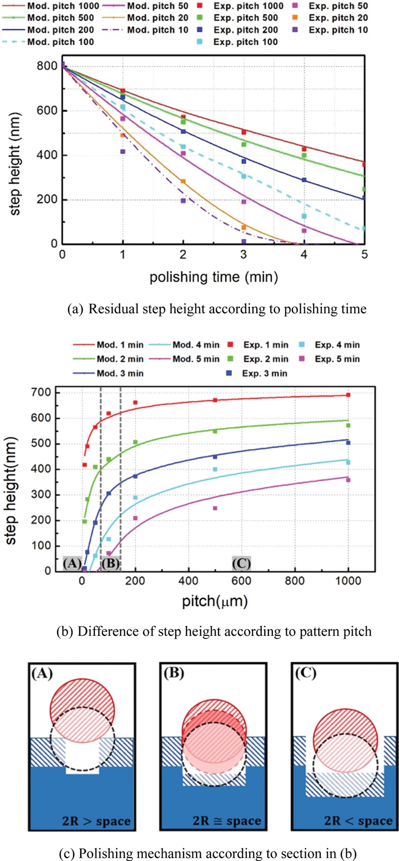
Fig. 12(a)는 패턴 크기에 따른 공정 시간별 단차 변화를 나타낸 그래프이다. 선의 경우 모델식에 대한 시뮬레이션 결과를 나타낸 것이며 점의 경우 실험 결과값을 나타낸다. 같은 공정 시간에 대한 피치별 잔여 단차를 비교하였을 때 피치가 작을수록 단차가 낮다는 것을 알 수 있으며 단차 제거 속도가 빨라진다는 것을 확인할 수 있다.
Fig. 12(b)의 경우 같은 데이터에 대해 공정 시간에 따른 패턴 크기별 단차의 변화를 확인할 수 있도록 나타낸 그래프이다. 그래프의 가장 특징의 경우 특정 크기를 기준점으로 연마 경향이 달라진다는 것을 알 수 있다. 약 100 μm를 기준점으로 그보다 작은 패턴의 경우 패턴의 크기가 작아질수록 잔여 단차가 기하급수적으로 작아지는 반면 그보다 큰 패턴 간의 비교를 할 경우 약간의 변화는 존재하나 크기에 따른 단차에 큰 차이가 없다는 것을 알 수 있다.
Fig. 12(c)는
Fig. 12(b)에서 나눈 구간 (A)부터 (C)에 대하여 연마 경향을 나타낸 모식도로, 같은 크기의 단일 돌기에 대하여 패턴의 크기에 따라 하부 연마의 차이에 대해 나타낸다. 2.3장 및 3.3장에서 언급했듯이 패턴의 크기에 따라 하부에 도달할 수 있는 돌기의 반경은 달라지며 그에 따라 하부 연마에 참여할 수 있는 돌기의 비율 역시 달라지게 된다. 다시 말하자면 구간 (A) 내의 경우 하부 연마가 거의 일어나지 않고 상대적으로 상부 연마만이 발생하므로 단차 제거 속도가 빠른 반면, 돌기보다 피치가 큰 구간 (C)의 경우 단차가 감소함에 따라 하부의 재료제거율이 점점 증가하여 상하부 연마가 동시에 진행되어 상대적으로 단차 제거가 더디게 진행되는 결과가 나타난다.
식(62)로부터 상하부의 연마량을 통해 얻은 잔여 단차에 대하여 평균 제곱근 오차는 약 19.84 nm를 가진다.
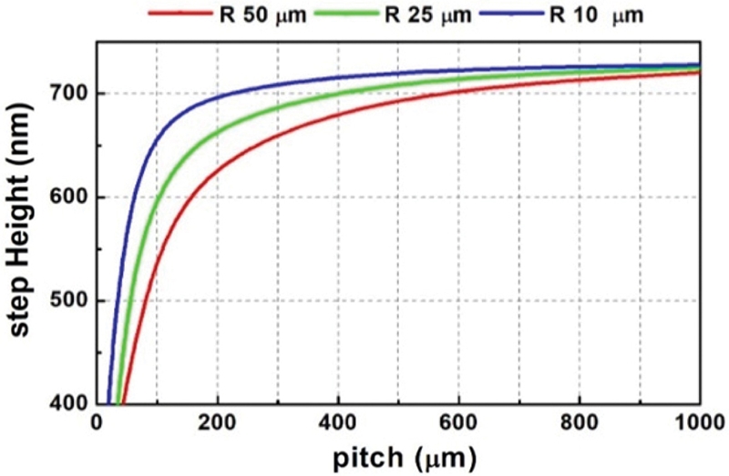
Fig. 12(b)의 (B)를 전후로 연마 경향이 변하는 결과에 대하여 분석하기 위해 돌기 반경을 변화시켜 패턴 크기별 단차에 대하여 비교해보았다.
Fig. 12Graphs of theoretical value vs. experimental value and polishing mechanism according to pattern pitch

Fig. 13은 모델식에 대하여 돌기의 곡률 반경을 변화시켜 돌기의 곡률 반경이 연마 결과에 미치는 영향을 확인하기 위해 돌기 곡률 반경을 10, 25, 50 μm의 세 가지로 설정하여 2분간 연마했을 경우 연마 결과를 시뮬레이션 한 결과를 나타낸 그래프이다.
Figs. 12(a) 및
12(b)에 대한 결과를 참고하여 이를 분석하자면 그래프에서 확인할 수 있듯이 돌기 반경이 감소함에 따라 연마 경향이 변하는 기준점이 그래프에서 왼쪽으로 이동하게 된다. 다시 말하자면 돌기 반경이 작아질수록 피치가 작은 패턴 영역에서도 패턴의 상하부 연마의 동시 진행이 보다 쉽게 일어날 수 있음을 알 수 있다. 이는
Γ, 즉 패턴의 하부 영역의 연마에 참여할 수 있는 돌기의 비율이 돌기 곡률 반경이 감소할수록 증가한다는 것을 의미하며
Γ이 증가함에 따라 상대적으로 작은 피치의 패턴에서도 동시 연마가 쉽게 진행되므로 단차 제거 속도가 빨라지는 구간이 왼쪽으로 옮겨진다는 것을 알 수 있다.
Fig. 13Residual step height according to the pitch for different asperity radius
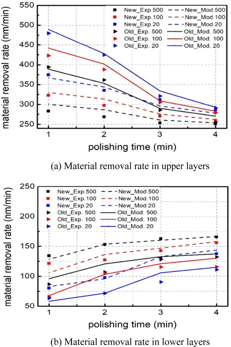
한편, 실제 공정에서는 패드의 마모가 진행됨에 따라 돌기 곡률 반경뿐만 아니라 돌기 높이 분포의 변화가 발생한다. 패드의 마모에 따른 기하학적 변화에 본 모델이 적절한 정합성을 갖추는지 확인하기 위해 새 연마 패드와 오랜 사용으로 마모가 진행된 패드를 각각 사용하여 산화막 패턴 웨이퍼를 1분에서 4분간 연마한 후 상하부층 각각의 재료제거율을 측정하였다.
Fig. 14는 패턴 피치에 따른 재료제거율을 나타낸 것으로
Fig. 14(a)는 상부층의 재료제거율,
Fig. 14(b)는 하부층의 재료제거율을 의미한다. 상부층의 재료제거율의 경우 패턴 사이즈가 작을수록 높아지며, 새 패드에 비해 마모된 패드를 사용하였을 때 높은 연마율을 나타낸다. 반면, 하부층의 재료제거율의 경우 패턴 사이즈가 작을수록 낮아지며, 마모된 패드에 비해 새 패드를 사용하였을 때 연마율이 높다는 것을 알 수 있다. 이는 같은 실험 조건하에 사용되는 패드의 기하학적 특성의 변화가 연마 결과에 크게 영향을 미치며, 특히 단차가 존재하는 패턴 웨이퍼의 경우 상하부의 연마율의 차이를 보다 크게 일으키는 결과를 초래하는 것을 알 수 있다. 본 모델을 통해 얻은 재료제거율과 실제 공정 데이터를 활용해 구한 재료제거율을 비교하였을 때 RMSE는 상하부 각각 16.58, 17.33 nm/min으로 높은 정합성을 가지는 것을 확인하였다.
Fig. 14Material removal rate according to pattern pitch with new and used pads

5. 결론
본 연구에서는 CMP 패드 돌기의 공정 시간에 따른 마모에 의한 돌기 높이 분포 변화와 패턴 웨이퍼 간의 접촉 메커니즘을 고려하여 재료제거율에 대한 수학적 모델을 제시하고 이에 대한 정합성을 분석하기 위해 실험을 진행하였다. 패턴의 피치가 감소함에 따라 단차 제거가 빠르게 진행되며 특히 특정 크기 전후로 연마 경향이 눈에 띄게 변화하는 것을 확인하였다. 돌기 직경 이하 크기의 미세 패턴 간의 비교에서는 피치가 감소할수록 단차 제거 속도가 급격히 빨라지는 경향을 보이는 반면 돌기 직경보다 큰 패턴의 경우 단차 제거 속도에 큰 차이가 나타나지 않았다. 또한 패드의 마모에 따른 기하학적 특성의 변화에 따라 재료제거율에 큰 영향을 미치는데, 새 패드에 비해 돌기 곡률이 작고 평균 돌기 높이 및 편차가 낮은 마모된 패드를 사용하였을 경우 상부층에서는 보다 높은 재료제거율을, 하부층에서는 보다 낮은 재료제거율로 연마가 진행되는 실제 결과를 본 모델을 통해 높은 정합성으로 예측할 수 있음을 확인하였다. 본 모델의 시뮬레이션 및 실험 결과와 같이 패턴의 형상과 돌기 크기의 상관관계에 따라 불균일한 연마 결과가 발생하는데, 이는 패턴의 크기에 따라 적합한 패드는 다르다고 볼 수 있다. 다시 말하자면, 대면적 크기의 패턴에 비해 미세 패턴의 경우 해당 패턴에 대해 하부 영역에 접촉할 수 있는 돌기의 크기 및 높이에 제한이 발생하게 되므로 돌기의 기하학적 특성에 더 큰 영향을 받게 된다. 패턴 크기의 영향으로 칩 내에서 발생하는 연마 불균일을 감소시키기 위해서는 무엇보다도 미세 패턴 영역에서 발생하는 이러한 영향을 줄이는 것이 필요하며, 이러한 문제점을 해결하기 위해서는 칩 내에 존재하는 패턴의 최소 피치를 고려하여 돌기의 기하학적 특성에 크게 제한 받지 않도록 설계된 패드 개발이 필요하며, 이러한 연구 개발에 있어 본 연구의 활용도 기대할 수 있다.
그러나 본 연구에서는 컨디셔닝 공정을 배제하고 모델링을 진행하였으나, 실제 CMP 공정에서는 연마 중 컨디셔닝을 함께 실시하는 것이 대부분의 경우이다. In-Situ의 경우에 대하여 모델을 적용하기 위해서는 컨디셔닝이 패드 거칠기의 변화에 주는 영향을 고려하여 돌기 높이 분포를 새롭게 정의하여 이를 확률 밀도 함수 유도에 적용한다면 보다 정확한 예측을 실시할 수 있을 것이다. 또한 실제 공정의 경우 슬러리의 입자가 연마에 참여하나, 본 연구의 모델의 경우 슬러리의 연마 입자의 크기를 완전히 무시하고 패드와 웨이퍼의 접촉 메커니즘에 초점을 두고 모델링을 진행하였다. 실제 공정과 가깝게 연마 입자가 기계적 연마에 미치는 영향을 적용하기 위해서는 입자의 크기를 고려하여 패드-입자-웨이퍼 간의 접촉을 정의하는 것이 필요하다.
ACKNOWLEDGMENTS
이 과제는 부산대학교 기본연구지원사업(2년)에 의해 연구되었음.
REFERENCES
- 1.
Liu, R., Pai, C. S., and Martinez, E., “Interconnect Technology Trend for Microelectronics,” Solid-State Electronics, Vol. 43, No. 6, pp. 1003-1009, 1999.
10.1016/S0038-1101(99)00015-5
- 2.
Lee, H. and Sung, I. H., “Chemical Mechanical Polishing: A Selective Review of R&D Trends in Abrasive Particle Behaviors and Wafer Materials,” Tribology and Lubricants, Vol. 35, No. 5, pp. 274-285, 2019.
- 3.
Lee, B., “Modeling of Chemical Mechanical Polishing for Shallow Trench Isolation,” Ph.D. Thesis, Massachusetts Institute of Technology, 2002.
- 4.
Boning, D., Lee, B., Oji, C., Ouma, D., Park, T., et al., “Pattern Dependent Modeling for CMP Optimization and Control,” MRS Online Proceedings Library Archive, Vol. 566, 1999.
10.1557/PROC-566-197
- 5.
Kasai, T., Anjur, S., Siriwardane, H., and Feeney, P., “Modeling for Pad Wear Control during Conditioning in CMP,” Proc. of the International Conference on Planarization/CMP Technology, pp. 1-6, 2007.
- 6.
Vlassak, J., “A Model for Chemical-Mechanical Polishing of a Material Surface based on Contact Mechanics,” Journal of the Mechanics and Physics of Solids, Vol. 52, No. 4, pp. 847-873, 2004.
10.1016/j.jmps.2003.07.007
- 7.
Tang, B. D., “Characterization and Modeling of Polysilicon MEMS Chemical-Mechanical Polishing,” M.Sc. Thesis, Massachusetts Institute of Technology, 2004.
- 8.
Vasilev, B., Rzehak, R., Bott, S., Kücher, P., and Bartha, J. W., “Greenwood-Williamson Model Combining Pattern-Density and Pattern-Size Effects in CMP,” IEEE Transactions on Semiconductor Manufacturing, Vol. 24, No. 2, pp. 338-347, 2011.
10.1109/TSM.2011.2107756
- 9.
Kim, H., Pak, B., Jeong, S., Lee, D., and Jeong, H., “Planarization Modeling based on Contact Mode between Pad Asperity and Oxide Pattern during CMP,” Journal of the Korean Society for Precision Engineering, Vol. 36, No. 4, pp. 363-372, 2019.
10.7736/KSPE.2019.36.4.363
- 10.
Greenwood, J. A. and Williamson, J. P., “Contact of Nominally Flat Surfaces,” Proceedings of the Royal Society of London. Series A, Mathematical and Physical Sciences, Vol. 295, No. 1442, pp. 300-319, 1966.
10.1098/rspa.1966.0242
- 11.
Babu, S., “Advances in Chemical Mechanical Planarization (CMP),” Elsevier, pp. 417-432, 2016.
- 12.
Golden, J., “The Evolution of Asperity Height Distributions of a Surface Subjected to Wear,” Wear, Vol. 39, No. 1, pp. 25-44, 1976.
10.1016/0043-1648(76)90220-9
- 13.
Borucki, L., “Mathematical Modeling of Polish-Rate Decay in Chemical-Mechanical Polishing,” Journal of Engineering Mathematics, Vol. 43, Nos. 2-4, pp. 105-114, 2002.
10.1023/A:1020305108358
- 14.
Vasilev, B., Bott, S., Rzehak, R., Liske, R., and Bartha, J. W., “A Method for Characterizing the Pad Surface Texture and Modeling its Impact on the Planarization in CMP,” Microelectronic Engineering, Vol. 104, pp. 48-57, 2013.
10.1016/j.mee.2012.10.007
- 15.
Preston, F., “The Theory and Design of Plate Glass Polishing Machines,” Journal of Glass Technology, Vol. 11, No. 44, pp. 214-256, 1927.
- 16.
Kim, S., Saka, N., and Chun, J. H., “The Effect of Pad-Asperity Curvature on Material Removal Rate in Chemical-Mechanical Polishing,” Procedia CIRP, Vol. 14, pp. 42-47, 2014.
10.1016/j.procir.2014.03.014
- 17.
Stein, D., Hetherington, D., Dugger, M., and Stout, T., “Optical Interferometry for Surface Measurements of CMP Pads,” Journal of Electronic Materials, Vol. 25, No. 10, pp. 1623-1627, 1996.
10.1007/BF02655586
Biography
- Somin Shin
M.Sc. candidate in the Department of Mechanical Engineering, Pusan National University. Her research interest is mathematical modeling of planarization with pad asperity property in CMP.
- Dasol Lee
Ph.D. candidate in the Department of Mechanical Engineering, Pusan National University. Her research interest is analysis of CMP mechanism and slurry supply system.
- Seonho Jeong
Ph.D. candidate in the Department of Mechanical Engineering, Pusan National University. His research interest is planarization modeling and analysis of pad asperity in CMP.
- Kyeongwoo Jeong
M.Sc. candidate in the Department of Mechanical Engineering, Pusan National University. His research interest is semiempirical modeling of planarization in CMP.
- Jinuk Choi
M.Sc. candidate in the Department of Mechanical Engineering, Pusan National University. His research interest is a model of pad temperature distribution during CMP.
- Haedo Jeong
Professor in the Department of Mechanical Engineering, Pusan National University. His research interest is CMP, grinding, polisher development and post-CMP cleaning.