ABSTRACT
With the increasing interest in research on the development of next-generation technologies such as flexible smartphones, displays, and wearable devices, interest in the development of materials and processes for transparent electrodes constituting them is also increasing. The most widely used material for manufacturing transparent devices is indium tin oxide (ITO). However, ITO is scarce, expensive, and brittle, making it is essential to replace it with new materials. In this study, we successfully fabricated a transparent electrode by electrospinning polyvinylpyrrolidone (PVP) and copper electroless deposition on the polyimide film. Especially, this study suggests a new combined heat treatment that uses both the hot plate and the convection oven. Through the combined heat treatment, the junctions between the nanofibers overlapped removed consequently reducing contact resistance. The mechanical stability of the fabricated electrode was evaluated by using a highly repeated bending test. Also, through the tape-peeling test, we confirmed that the adhesive strength of the electrode was high. This method can be applied to various polymer-based, substrate which are vulnerable to annealing process.
-
KEYWORDS: Transparent electrode, Electrospinning, Electroless plating, Heat treatment
-
KEYWORDS: 투명 전극, 전기 방사, 무전해 도금, 열처리
1. 서론
최근, 장소와 시간에 관계없이 사용자가 자유롭게 네트워크에 접속할 수 있는 유비쿼터스 시대가 되고 있음에 따라 휴대가 간편하고 이동성을 갖는 웨어러블 디바이스의 필요성이 대두되고 있다. 또한 의료 및 헬스케어 목적의 웨어러블 디바이스의 관심이 증가하여 관련 시장이 급격히 성장하고 있다. 웨어러블 디바이스 개발 연구가 활발히 이루어지는 가운데 이들을 구성하는 투명 전극의 소재 및 공정 개발에 대한 관심 또한 나날이 높아지고 있다. 투명 전극이란 높은 전도도와 가시광선 영역의 높은 투과도 특성을 갖는 전극이다. 현재 상용화된 투명 디스플레이 및 각종 센서의 제작에 현재 가장 활발히 사용되는 물질은 인듐 주석 산화물(ITO)이다. 하지만 ITO는 희소성이 높고 가격이 비싸며, 취성이 높아 유연 소자의 생산에 부적합하다. 이에 따라 ITO를 대체할 수 있는 재료와 그에 상응하는 공정에 대한 개발이 필요한 상황이다.
나노 섬유는 일반적으로 분무법, 플라즈마 강화 화학 기상 증착법, 기판법 등의 방법을 이용하여 제조되어 왔다
[1]. 그러나 이러한 방식들은 매우 복잡하고 비용이 많이 들며 생산 속도가 느려 나노 섬유의 대량생산 방식으로는 적합하지 않다. 전기 방사 공정은 정전기력을 이용하여 고분자 용액에 전하를 발생시키고, 표면 장력보다 큰 전기력을 표면에 가할 때 젯(Jet)에서 용액이 분무되며 나노 섬유가 생산되는 원리이다. 기존 방식으로 생산된 섬유보다 전기 방사 공정을 통해 생산된 섬유가 Nano-micro Scale로 더 얇은 직경을 가지며 더 큰 표면적을 갖는다
[2]. 또한 적은 양의 폴리머 용액으로도 나노 섬유의 대량 생산이 가능하기 때문에 경제적이며, 간단하고 빠른 공정이다. 전기 방사는 보통 상온, 상압의 조건에서 진행되므로 복잡한 진공 공정이 필요 없다는 장점이 있다. 전기 방사로 생산된 섬유는 센서, 에너지 저장 및 변환, 조직 공학 등 다양한 분야에 적용되고 있다
[3-
6]. 이처럼 기존 제조 방식의 문제점들을 해결할 수 있는 전기 방사 공정이 투명 전극의 제조 방법으로서 점차 많이 채택되고 있다.
투명 전극은 약 1,000 Ω/sq 이하의 면저항 특성을 나타내야 하는데 적층 방식의 전기 방사 공정 시 발생하는 나노 섬유 사이에서의 겹침 현상, 다시 말해 Junction의 발생은 전극의 높은 전기적 저항으로 이어진다는 문제가 발생한다
[7]. 이러한 나노 섬유 간의 접촉 저항은 일반적으로 가열, 용매, 전류 등을 통해 제거된다
[8-
10].
본 연구에서는 PI (Polyimide) Film 위에 전기 방사된 팔라듐 (Palladium) 촉매를 함유한 나노 섬유를 핫 플레이트와 대류 오븐을 이용하여 두 차례의 열을 순서대로 가하는 복합 열처리 방식으로 Junction-free 형상을 제작하였다. 기존의 선행 연구에서는, 핫 플레이트를 통해 500-600oC의 열을 직접적으로 가해 전기 방사된 나노 섬유 간 발생하는 접합점(Junction)을 제거하였다. 그러나 열변형 온도가 비교적 낮은 PET (Polyethylene Terephthalate), PU (Polyurethane), PI (Polyimide) 등의 폴리머 필름을 기판 소재로 사용할 경우, 이 과정에서 기판 상에 열이 직접적으로 전도되어 표면 손상 문제가 발생하였다. 따라서 본 연구에서는 핫 플레이트를 사용한 열처리 공정의 온도를 300oC로 낮추었으며, 이후 오븐의 대류 현상을 이용하여 200oC 가량 추가적인 열을 가해줌으로써 고온의 열이 직접 전도되며 발생하던 필름의 표면 손상 문제를 해결함과 동시에 전극의 도금 안정성과 전도성을 높였다. 또한, 무전해 도금은 물체의 크기 및 소재에 제한을 받지 않고 외부 전원 없이 화학 반응을 통해 도금이 가능한 장점을 가지고 있다.
기존 연구에서는 나노 섬유 네트워크의 표면적, 접착성 및 다공성을 향상시키기 위하여 화학적 활성화, 플라즈마 및 산처리 등 별도의 추가 공정을 사용하였다
[11-
13]. 높은 표면적은 Intercalation과 Deintercalation이 동시에 이루어짐으로써 층간 간격이 부분적으로 가스화되고 확장되었기 때문에 발생한다
[14]. KOH, NaOH와 같은 알칼리 화합물을 이용한 화학적 활성화는 표면적이 큰 탄소 재료를 활성화시키는 잘 알려진 방법이다. 또한, 특정 용매의 사용, 습도 환경의 변화, 폴리머 혼합물을 사용하는 방법 등을 사용하여 방적된 나노 섬유에 기공을 미리 생성한 다음 열을 사용하여 다공성을 높일 수도 있다
[15]. 하지만 이 연구에서는 별도의 활성화 장치나 추가 공정 없이, 단순히 두 번의 열처리를 통해 필름 표면의 팔라듐을 활성화하여 비용을 절감하고 시간 손실을 해결할 수 있는 결과를 도출하였다. 금속 네트워크에 기계적 및 열적 응력을 가하지 않고, 단순히 열을 추가로 가해 접합 없는 나노 섬유 네트워크 형태를 만들어 공정을 간소화했으며, 이러한 과정은 금속 구성 요소의 특성에 영향을 미치지 않았다.
본 연구는 열에 취약한 폴리머 기판에 전기적으로 안정적인 특성의 투명 전극의 제작을 목적으로 하였다. 이를 위해, PVP (Polyvinylpyrrolidone) 나노 섬유를 전기 방사 공정을 통해 생산하고, 두 차례의 복합 열처리 공정을 통해 접합을 제거한 후, 이를 구리로 무전해 도금하여 최종적으로 안정성이 높은 금속 전극을 제작하였다. 복합 열처리를 통하여 나노 섬유 간의 Junction을 효과적으로 제거하여 필름 표면 손상 문제를 해결하였으며 접촉 저항 및 투과도를 개선하였다. 복합 열처리를 적용한 금속 전극은 기존 열처리 적용 전극에 비해 약 70% 향상된 투과도와 93% 향상된 면저항을 보였다.
2. 실험 재료 및 실험 과정
2.1 실험 재료
실험에 사용된 Polyimide films, Poly (vinylpyrrolidone) (PVP, AR, molecular weight, 1,300,000) Powder, Copper (II) Sulfate Pentahydrate (CuSO4-5H2O, special grade, 99.5%), N, N-dimethylformamide (DMF, special grade, 99.5%), Sodium hydroxide (NaOH, special grade, 98.0%), Ammonium Tetrachloropalladate (II) ((NH4)2PdCl4, 99.998% (Metals basis)), Potassium sodium (+) – tartrate tetrahydrate (KNaC4H4O6-4H2O)는 Sigma-Aldrich (USA)를 통해, Formaldehyde (HCHO) solution (36.0-38.0%) 은 Wako Pure Chemical Industries, Ltd. (Japan)을 통해 구매하였고, 모든 시약은 정제없이 사용되었다.
2.2 실험 장비
Field Emission Scanning Electron Microscope (FE-SEM)를 이용해 구리 나노 섬유의 형상을 관찰하였다. ImageJ (NIH, USA) 프로그램을 이용해 구리 입자 분포 면적 및 나노 섬유의 두께를 측정하였다. Ultraviolet-visible (UV Vis) Spectrophotometry (OPTIZEN POP-V; JASCO, Japan)를 이용해 투과도를 측정하였으며 기준 투과율은 Bare PI film의 투과율이었다. 금속 전극의 면저항은 4점 프로브(CMTSR2000N; AIT Co., Ltd., Korea)를 사용하여 측정되었다.
2.3 실험 과정
2.3.1 팔라듐 촉매층 형성
PI film 표면은 소수성을 띄기 때문에, 이로 인해 표면 접착력이 낮다는 성질을 갖는다
[16]. 고분자 필름과 금속층 간의 접합성 증대를 위한 산소 플라즈마 처리를 통해 PVP-Pd Solution의 안정적인 전기 방사를 유도하였다. 플라즈마 공정은 100 W로 2분 동안 진행되었다(
Fig. 1(A)). 팔라듐 이온이 함유된 PVP 기반의 폴리머 용액을 표면 개질 처리된 PI film 위에 전기 방사하여 섬유를 생산하였다. 10 kV의 전압이 인가되었으며 집전체와 제트 방출원 사이의 거리를 15 cm로 설정하였고, 고분자 용액에 대하여 5 μL/min의 유량으로 기판에 20초 동안 나노 섬유를 증착 하였다. 전기 방사 시 상대습도 및 온도는 각각 40-50 RH%, 22-23
oC로 유지하였다(
Fig. 1(B)). 전극의 성능을 저해하는 섬유 간의 겹침 현상은 두 차례로 나뉘어 가해지는 열을 통해 효과적으로 제거된다. 1차적으로 공기 중의 핫 플레이트를 이용하여 PI film 기판에 열을 직접 가한다. 300
oC의 온도로 PVP 나노 섬유가 방사된 기판을 30분 동안 열처리하여 무전해 도금을 위한 팔라듐 시드 레이어(Palladium Seed Layer)를 형성하였고 동시에 기판 위의 섬유 안정화가 시작되었다(
Fig. 1(C)). 도금 안정성과 전극의 균일한 성능을 위해 대류 오븐을 통해 시편의 표면에 추가로 열을 가한다. 200
oC의 온도로 30분 동안 추가적인 열처리가 진행된다. 두 차례의 복합적인 열처리 공정을 통해 섬유 안정화가 완료되었고 금속 도금 환경이 조성되었다(
Fig. 1(D)).
Fig. 1The schematic of fabrication process for a metallic network (A) Preparation of polyimide film after oxygen plasma treated (B) Electrospinning PVP nanofiber onto PI film (C) First heat treatment using hotplate (D) Second heat treatment using convection oven (E) Copper electroless deposition (F) Wiring
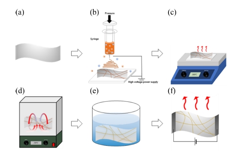
2.3.2 구리 무전해 도금
전기 방사 및 열처리 공정을 통해 형성된 팔라듐 시드 레이어를 도금 용액에 침지시켜 구리 무전해 도금 공정을 진행하였다. 이 때, 구리 무전해 도금 용액의 조성은 다음과 같다; DI water를 기준으로 하여 Formaldehyde, Sodium Hydroxide, Potassium Sodium (+) - Tartrate Tetrahydrate, Copper (II) Sulfate Pentahydrate를 각각 0.1, 40, 140, 30 mg/mL를 넣고 Magnetic Stirrer를 사용해 500 RPM으로 1시간 동안 교반한다. 이 때, Formaldehyde는 전자를 공급해주는 환원제로, Sodium Hydroxide pH 조절제, Potassium Sodium (+) - Tartrate Tetrahydrate는 착화제, Copper (II) Sulfate Pentahydrate 구리 금속 이온을 공급해주는 역할을 한다. 구리 무전해 도금의 화학적 반응식은
식(1)과 같다;
팔라듐 촉매에 의한 구리 무전해 도금을 2분 동안 진행한 후 탈이온수로 세척하여 마무리한다(
Fig. 1(E)). 별도의 활성화 과정 없이 단순 열을 가해주는 것으로 금속 전극을 제작하는 과정을 단순화하였다(
Fig. 1(F)).
3. 실험 결과 및 분석
3.1 열처리 방식에 따른 나노 섬유 형상 분석
Fig. 2는 FE-SEM을 통해 단일 열처리, 복합 열처리 공정을 거쳐 제조된 금속 전극의 나노 섬유를 고배율(30,000배) 로 관찰한 것이다. PVP가 함유된 고분자 용액을 PI film 기판 위에 직접 전기 방사하여 시드층을 생산하였고 그 후 열처리 과정과 무전해 도금을 통해 방적된 섬유를 금속화하였다. 시드층 내에 포함된 팔라듐 이온은 촉매로 사용되며, 구리 무전해 도금을 통해 구리 이온이 침전되어 구리 나노 섬유를 형성한다.
Fig. 2(A)는 전기 방사 직후의 나노 섬유 형상을 나타낸다.
Figs. 2(B)-
2(F)는 PI film의 용융점을 고려해 기존 연구에서 진행하던 단일열처리 공정의 시간을 변수로, 15분 간격으로 구리 나노 섬유의 형태적 변화를 관찰한 사진이다. 300
oC의 온도로 핫 플레이트를 이용하여 기판에 직접적으로 열처리를 가하는 단일 열처리 진행 시간이 30분 미만인 경우에는 열이 충분한 시간동안 가해지지 않아 섬유가 활성화되지 못하였으며 그 결과로 섬유의 금속화가 실패하였음을
Fig. 2(B)를 통해 확인할 수 있다. 열처리 시간이 증가함에 따라 섬유의 활성 정도 또한 증가하는 추세를 보였으나, 열처리 공정을 30분 동안 진행했던
Fig. 2(C)는 PVP 나노 섬유의 일부분만이 무전해 도금 진행되어 비교적 낮은 균일성를 보였다. 45분의 단일 열처리 및 무전해 도금 결과, 금속 전극의 도금 안정성은
Figs. 2(C)와
2(D)의 섬유에 비해 확연히 증가하였음을
Fig. 2(E)를 통해 확인할 수 있다. 그러나 무전해 도금 전 열처리 공정의 진행 목적 중 하나였던 나노 섬유 접합부의 중첩이 제거되지 않았음이 확인되었다. 따라서 단일 열처리 공정을 통해 Junction-free 형상을 제작함과 동시에 높은 전기 전도성 및 균일성을 갖는 금속 전극을 제조하기 위해서는 60분 이상의 장시간의 열처리 시간이 필연적임을 알 수 있다. 그러나 필름의 표면에 고온의 열이 직접적으로 가해지는 기존 열 처리 방식 특성상 이는 전극의 손상을 유발한다는 문제가 발생한다. 이는 전극의 저항 증가와 전도성 저하로 이어지며 기판의 소재 또한 제한된다. 이러한 문제를 해결하기 위해 본 연구에서는 핫 플레이트를 사용하여 표면에 직접 열을 가하는 시간을 단축하고, 그 후에는 대류 오븐을 이용하여 고온 바람을 추가로 가하는 방식을 적용하여 열처리 방법을 복합적으로 진행하였다. 그 결과, 단일 열처리를 60분 실시한 시편(
Fig. 2(E))에서 발생한 나노 섬유의 융용 현상이 복합 열처리 시편(
Fig. 2(F))에서는 사라졌음을 확인할 수 있다. 또한, 무전해 도금 과정에서 발생하는 나노 섬유 주변의 구리 입자들도 효과적으로 제거되었다.
Fig. 2FE-SEM images of metallic network depending on the time and conditions of heat treatment (A) Electrospun nanofibers (B-E) Single heat-treated metallic network for 15, 30, 45, 60 min, respectively (F) Combined heat-treated metallic network
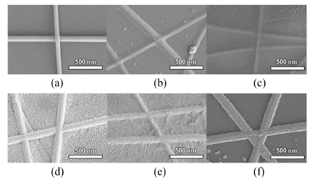
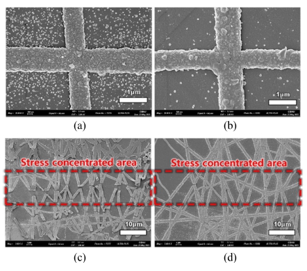
Fig. 3 는 FE-SEM을 통해 단일 열처리, 복합 열처리 공정을거쳐 제조된 금속 전극의 나노 섬유를 고배율(20,000배)로 관찰한 것이다.
Figs. 3(A)와
3(B)는 각각 단일 열처리 30분과 복합 열처리를 거친 시료의 구리 금속화 결과이며,
Figs. 3(C)와
3(D)는 각각의 조건의 나노 섬유에 기계적 힘을 가한 뒤 생긴 Crack(균열) 형상을 나타낸다. 이 때, 기계적 힘은 5 kg의 무게추를 통해 1분간 인가되었으며 가해진 압력은 약 49.05 kPa이다. 나노 섬유 네트워크 위의 균열 정도와 형태를 확인하였을때 복합 열처리를 거친 섬유 보다 단일 열처리를 거친 섬유에서 섬유의 끊김 현상이 더 빈번하게 발생하였으며 이는 열처리 방식의 변화로 균열 저항성이 높아졌음을 의미한다. 또한 무전해 도금을 통한 금속화가 더 높은 수준으로 진행되었음을 의미한다. 기계적 힘 인가를 통한 균열 형상 비교를 통해 복합 열처리 공정이 기판과 나노 섬유 사이의 접합 강도가 높아질 수 있음을 확인하였다
[17].
Fig. 3Comparison of single heat and combined heat-treated metallic network with FE-SEM images (A) Single heat-treated for 30 min metallic network (B) Combined heat-treated metallic network (C) Crack image of single heat-treated metallic network after applying stress (D) Crack image of combined heat-treated metallic network after applying mechanical stress

본 연구에서는 금속 나노 섬유의 안정적인 생산과 재현성 향상을 위해 30 wt% 농도의 폴리머 용액을 사용하여 전기 방사를 수행하였으며, 폴리머 나노 섬유의 안정화를 위하여 열처리 방법을 적용하였다
[18]. 열처리는 폴리머의 열분해를 통해 분자 구조의 변화와 결정화를 유도하여 나노 섬유의 안정성을 증가시킨다
[19]. 공기 중의 핫 플레이트에서 1차적으로 섬유의 안정화를 시작한다. 섬유 간의 겹침 구조에 가해진 열은 구조의 열 변성을 일으키며 최종적으로 대류 오븐에서 기판을 완전히 안정화 및 팔라듐 촉매층을 활성화하였다. 고정된 온도 및 습도 환경에서 시료 전반에 걸쳐 고르게 열이 가해지는 과정은 금속 전극이 비교적 균일한 성능을 갖게 한다. 또한 열처리된 촉매층에 금속이 도금되기 때문에 기판과 전도성 네트워크 사이의 접착 강도는 우수하다
[20].
Fig. 4는 전기 방사 및 무전해 도금 공정을 통해 제작한 금속 전극의 전기적, 광학적 및 기계적 특성을 나타낸 것이다.
Fig. 4(A)에서는 1차 열처리 시간 및 열처리 방식에 따른 구리 나노 섬유의 두께 차이를 확인할 수 있다. 나노 섬유 두께의 측정을 위해 SEM 이미지를 사용하였으며 섬유 두께의 분포는 각 조건에 대해 무작위로 5번 측정한 후 그들의 평균값을 통해 결정되었다. 단일 열처리가 적용된 구리 나노 섬유의 두께는 열처리 시간에 반비례하였으며 평균 두께는 128.75 nm이었고 각 15분씩 열을 추가로 가할 시 평균 0.2 nm/min의 속도로 점진적으로 나노 섬유의 두께가 감소함을 보인다. 복합 열처리의 나노 섬유 두께는 127.9 nm로 이는 열처리 방식이 나노 섬유의 두께 변화에 큰 영향을 미치지 않음을 나타낸다.
Fig. 4Electrical, optical, and mechanical analysis of fabricated metallic nanofiber network (A) Graph about Cu nanofiber thickness depending on the heat treatment time and method (B) Graph about heat treatment time and sheet resistance (C) Graph about transmittance for each heat treatment process (visible range: 600 to 900 nm) (D) Graph about sheet resistance strain depending on bending cycle number
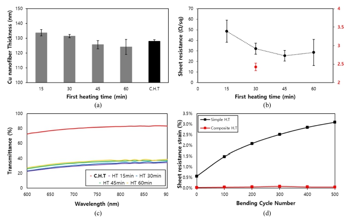
Fig. 4(B)는 핫플레이트를 사용한 단일 열처리 시간에 따른 면저항의 변화와, 핫플레이트와 대류 오븐을 사용한 복합 열처리 방식의 면저항을 측정한 결과를 보여준다. 단일 열처리 전극은 열처리 시간이 길어질수록 점차적으로 낮은 면저항을 나타내며, 이는 나노 섬유 간의 중첩이 제거되어 박막의 전도성이 점차적으로 증가하고 있음을 의미한다. 그러나, 일정 시간 동안의 열처리가 진행된 이후에는, 나노 섬유에 손상이 발생하기 시작하여 면저항은 다시 증가하였고 도금의 균일성 또한 감소함을 오차 막대를 통해 확인하였다. 단일 열처리 전극과 복합 열처리 전극의 평균 면저항은 각각 36.015, 2.425 /sq로 별도의 공정 없이 시료에 열을 가하는 방식을 변화함으로써 약 93% 개선됨을 확인하였다. 금속 나노 섬유 네트워크의 면저항은 구리 나노 섬유에 가해지는 열의 시간 및 방식을 변화시킴으로써 용이하게 제어할 수 있다.
Fig. 4(C)는 600-900 nm 파장 범위의 필름 기판 상에서 구리 나노 섬유의 투과 스펙트럼을 나타낸다. 열처리 방식에 무관하게 점차 증가하는 투과율을 보이나, 측정되는 수치는 열처리 방식에 따라 눈에 띄는 차이를 보였다. 단일 열처리 전극의 투과율은 평균 약 30%이었으나, 기존의 열처리에 오븐에 의한 추가 대류열을 가한 복합 열처리 전극의 투과율은 70%로 효과적으로 개선되었다. 이러한 결과는 무전해 도금 후 기판상의 구리입자의 면적 계산을 통해 확인할 수 있었다. 단일 열처리 공정을 통한 기판의 구리 입자 면적은 평균 46.1%로 나노 섬유주위로 넓게 분포되어 있었으나, 두 차례의 복합적인 열처리 방식을 통해 구리 입자의 면적을 18.5%로 감소시킴과 동시에 전극의 투과율 또한 증대시켰다.
Fig. 4(D)는 금속 전극의 Bending Cycle 수에 따른 면저항의 변화를 열처리 방식별로 나타낸 그래프다. 부면에 위치한 구리 나노 섬유 네트워크에 하중을 가하여 금속 전극을 500회 구부림으로써 측정하였다. Bending Cycle의 횟수가 증가함에 따라 단일 열처리 공정을 거친 전극의 면저항 변형률은 계속해서 증가하였으며, 0.506 %/cycle의 평균 증가율을 보였다. 이와 대비되게 복합 열처리 전극에 동일한 Bending Test를 진행한 경우에는 0.049 %/cycle로 단일 열처리 전극에 비해 약 10배 가량 낮은 면저항 증가율을 보였다. Cycle 내에서의 최대 변형률 값은 각각 11.45%와 3.413%로 약 70%의 저항 안정성을 확인할 수 있었다. 안정적인 금속 전극의 제작이 본 연구의 최종 목적이기에, 기존 열처리 후 진행되는 추가 열처리 공정은 유의미함을 나타낸다.
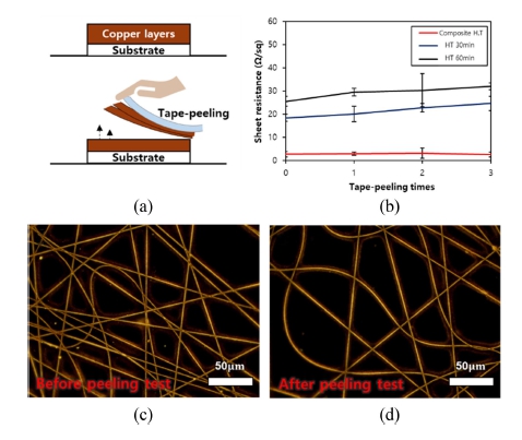
3.3 테이프 필링 시험에 따른 특성 분석
Figs. 5(A)와
5(B)는 Tape-peeling Test를 통해 PI film 위에 형성된 구리 금속층의 접착 성능을 테스트하는 과정을 나타낸 것이다. 성능을 효과적으로 확인하기 위하여 투명한 상용 3M Scotch Tape를 사용해 총 3차례의 Peeling Test를 시도하였다(테이프 시험에 의한 부착력 측정을 위한 표준시험방법, ASTM D3359-97). 열처리 30분과 60분 시료의 면저항은 3번의 박리 사이클 동안 면저항이 증가하였고, 각각 초기값 대비 테스트 전과 후 최대 34, 25%의 변화율을 보였다. 반면, 복합 열처리 공정을 거친 시료는 3회의 Tape-peeling 후에도 면저항에 거의 변화가 없었다. 이를 통해 열처리 방식에 따라 PI film과 구리 나노 섬유 간의 접합 강도 차이가 존재함을 확인하였다. 이전 연구에서 제기된 전도성 필름 장치와 기판 간의 낮은 접착 한계는 별도의 다른 공정 없이 열처리 방식을 변경함으로써 해결되었으며 PI 기판과 구리 금속층 사이의 기계적 접착 강도를 향상시켰다
[21].
Figs. 5(C)와
5(D)는 각각 복합 열처리를 거친 구리 금속층의 Tape-peeling 이전과 이후의 형상 변화를 광학 현미경으로 관찰한 사진이다. Tape-peeling 이후에도 박리된 나노 섬유를 발견할 수 없으며, 금속 나노 섬유의 형상의 변화도 나타나지 않았다. 이는 나노 섬유와 기판 사이의 접합력이 견고함을 나타낸다.
Fig. 5(A)The schematic of tape peeling test (B) Graph about the sheet resistance depending on the times of tape-peeling test (C) Optical image of metallic network before tape-peeling test (D) Optical image of metallic network after tape-peeling test
4. 결론
본 연구에서는 두 차례의 복합적인 열처리 공정을 통한 금속 전극 제작 방법을 제시하였다. 무전해 도금 공정에서 별도로 진행되던 활성화 과정을 생략하고 기존 공정 내에서 나노 섬유의 활성화를 이끌어냄으로써 공정을 단순화하였다. 오븐을 통한 복합 열처리 공정을 사용함으로써, 제작 공정 변화를 최소화하면서 전극의 전기적, 기계적 성능을 향상시켰다. 스트레인에 따른 균열의 발생과 Tape-peeling Test를 통해 기판과 전극사이의 접합력 증가를 확인할 수 있었으며, Bending Test를 통해 전극의 우수한 기계적 강도를 확인할 수 있었다. 특히, 본 제작 방법은 열에 매우 취약한 특성을 갖는 PU (Polyurethane), PET (Polyethylene Terephthalate), PDMS (Polydimethylsiloxane) 등의 고분자 기반에 적용 시 유연 소자 및 웨어러블 디바이스 등 그 응용 분야가 더욱 확장될 수 있을 것으로 기대된다.
ACKNOWLEDGMENTS
이 성과는 정부(과학기술정보통신부)의 재원으로 한국연구재단의 지원을 받아 수행된 연구임(No. NRF-2022R1G1A1007757).
이 논문은 2021년도 정부(과학기술정보통신부)의 재원으로 한국연구재단의 지원을 받아 수행된 연구임(No. 2021R1A4A1033141).
REFERENCES
- 1.
Alghoraibi, I., Alomari, S., (2018), Different methods for nanofiber design and fabrication, Handbook of Nanofibers, 1-46.
10.1007/978-3-319-42789-8_11-2
- 2.
Leijten, J., Rouwkema, J., Zhang, Y. S., Nasajpour, A., Dokmeci, M. R., Khademhosseini, A., (2016), Advancing tissue engineering: a tale of nano-, micro-, and macroscale integration, Small, 12(16), 2130-2145.
10.1002/smll.201501798
- 3.
Wang, X., Drew, C., Lee, S.-H., Senecal, K. J., Kumar, J., Samuelson, L. A., (2002), Electrospun nanofibrous membranes for highly sensitive optical sensors, Nano Letters, 2(11), 1273-1275.
10.1021/nl020216u
- 4.
Li, X., Zhi, L., (2018), Graphene hybridization for energy storage applications, Chemical Society Reviews, 47(9), 3189-3216.
10.1039/C7CS00871F
- 5.
Bhardwaj, N., Kundu, S. C., (2010), Electrospinning: A fascinating fiber fabrication technique, Biotechnology Advances, 28(3), 325-347.
10.1016/j.biotechadv.2010.01.004
- 6.
Zhang, X., Lu, Y., (2014), Centrifugal spinning: An alternative approach to fabricate nanofibers at high speed and low cost, Polymer Reviews, 54(4), 677-701.
10.1080/15583724.2014.935858
- 7.
Song, R., Li, X., Gu, F., Fei, L., Ma, Q., Chai, Y., (2016), An ultra-long and low junction-resistance Ag transparent electrode by electrospun nanofibers, RSC Advances, 6(94), 91641-91648.
10.1039/C6RA19131B
- 8.
Saito, T., Yamada, T., Fabris, D., Kitsuki, H., Wilhite, P., Suzuki, M., Yang, C. Y., (2008), Improved contact for thermal and electrical transport in carbon nanofiber interconnects, Applied Physics Letters, 93(10), 102108.
10.1063/1.2979710
- 9.
Li, G., Martinez, C., Janata, J., Smith, J. A., Josowicz, M., Semancik, S., (2004), Effect of morphology on the response of polyaniline-based conductometric gas sensors: Nanofibers vs. thin films, Electrochemical and Solid-state Letters, 7(10), H44.
10.1149/1.1795053
- 10.
Kim, B.-H., Yang, K. S., Kim, Y. A., Kim, Y. J., An, B., Oshida, K., (2011), Solvent-induced porosity control of carbon nanofiber webs for supercapacitor, Journal of Power Sources, 196(23), 10496-10501.
10.1016/j.jpowsour.2011.08.088
- 11.
Chen, Q., Dai, L., Gao, M., Huang, S., Mau, A., (2001), Plasma activation of carbon nanotubes for chemical modification, The Journal of Physical Chemistry B, 105(3), 618-622.
10.1021/jp003385g
- 12.
Wang, D., Liu, Z., Yue, Y., Xu, X., Cai, D., Han, C., Song, J., Xiao, J., Wu, H., (2021), Blow spinning of pre–acid-activated polyamidoxime nanofibers for efficient uranium adsorption from seawater, Materials Today Energy, 21, 100735.
10.1016/j.mtener.2021.100735
- 13.
Barranco, V., Lillo-Rodenas, M., Linares-Solano, A., Oya, A., Pico, F., Ibañez, J., Agullo-Rueda, F., Amarilla, J. M., Rojo, J., (2010), Amorphous carbon nanofibers and their activated carbon nanofibers as supercapacitor electrodes, The Journal of Physical Chemistry C, 114(22), 10302-10307.
10.1021/jp1021278
- 14.
Moon, S., Gil, M., Lee, K. J., (2017), Syringeless electrospinning toward versatile fabrication of nanofiber web, Scientific Reports, 7(1), 41424.
10.1038/srep41424
- 15.
Park, S.-J., Lee, H.-Y., (2005), Effect of atmospheric-pressure plasma on adhesion characteristics of polyimide film, Journal of Colloid and Interface Science, 285(1), 267-272.
10.1016/j.jcis.2004.11.062
- 16.
Jiu, J., Nogi, M., Sugahara, T., Tokuno, T., Araki, T., Komoda, N., Suganuma, K., Uchida, H., Shinozaki, K., (2012), Strongly adhesive and flexible transparent silver nanowire conductive films fabricated with a high-intensity pulsed light technique, Journal of Materials Chemistry, 22(44), 23561-23567.
10.1039/c2jm35545k
- 17.
Wiklund, U., Hedenqvist, P., Hogmark, S., (1997), Multilayer cracking resistance in bending, Surface and Coatings Technology, 97(1-3), 773-778.
10.1016/S0257-8972(97)00290-9
- 18.
Yousefzadeh, M., (2017), 12 - Modeling and simulation of the electrospinning process, Electrospun Nanofibers, Elsevier, 277-301.
10.1016/B978-0-08-100907-9.00012-X
- 19.
Enayati, M. S., Behzad, T., Sajkiewicz, P., Bagheri, R., Ghasemi-Mobarakeh, L., Łojkowski, W., Pahlevanneshan, Z., Ahmadi, M., (2016), Crystallinity study of electrospun poly (vinyl alcohol) nanofibers: Effect of electrospinning, filler incorporation, and heat treatment, Iranian Polymer Journal, 25(7), 647-659.
10.1007/s13726-016-0455-3
- 20.
Woo, H., Kim, S., Yoon, S., Kim, K., Kim, G. H., An, T., Lim, G., (2021), Highly flexible and transparent film heater with electrospun copper conductive network via junction-free structure, Journal of Alloys and Compounds, 886, 161191.
10.1016/j.jallcom.2021.161191
- 21.
Lasprilla-Botero, J., Alvarez-Lainez, M., Lagaron, J., (2018), The influence of electrospinning parameters and solvent selection on the morphology and diameter of polyimide nanofibers, Materials Today Communications, 14, 1-9.
10.1016/j.mtcomm.2017.12.003
Biography
- Na Kyoung Kim
M.Sc. candidate in the Department of Mechanical Engineering, Chungbuk National University. Her research interest is micro/ nano technology.
- So Eun Kim
B.Sc. candidate in the Department of Mechanical Engineering, Chungbuk National University. Her research interest is metallization of polymers.
- Doyeon Im
M.Sc. candidate in the Mechanical Design Engineering, Andong National University. Her research interest is nanoscience, nano fabrication, and MEMS.
- Seung Mi Hong
B.Sc. candidate in the Department of Mechanical Engineering, Chungbuk National University. Her research interest is materials of metallization process.
- Taechang An
Professor in the Department of Mechanical Robotics Engineering, Andong National University. His research interest is nanoscience, nano fabrication, microfluidics, and MEMS.
- Geon Hwee Kim
Professor in the Department of Mechanical Engineering, Chungbuk National University. His research interest is wearable device, MEMS, biosensor, and nano fabrication.