ABSTRACT
In this study, we demonstrate a synergistic enhancement of photoluminescence (PL) in an atomically thin molybdenum disulfide (MoS2) monolayer using a dual-laser-beam-assisted chemical modification method. A continuous-wave (CW) green laser, directed perpendicularly at the MoS2, locally raises the temperature and induces the formation of sulfur (S) vacancies, resulting in a significant increase in PL intensity. Subsequently, a UV nanosecond laser beam laterally illuminates the area above the MoS2 layer, breaking chlorine molecules and introducing chlorine radicals without damaging the sample. This process further enhances the PL in the region previously affected by S vacancies. The binding energy of chlorine atoms to S-vacancy sites is greater than that to the pristine MoS2 surface, facilitating more effective p-type doping. The stronger interaction at the defect sites created by the CW laser contributes to the observed synergistic PL enhancement. Our approach presents a novel method for precise and spatially selective chemical doping in two-dimensional (2D) van der Waals (vdW) materials.
-
KEYWORDS: Laser doping, 2D materials, Defect engineering, Chlorination, Photoluminescence
-
KEYWORDS: 레이저 도핑, 이차원 소재, 결함 조절, 염소화, 광발광
1. Introduction
2D transition metal dichalcogenides (TMDCs), such as MoS
2 and WS
2, have gained much attention as promising materials for next-generation electronics and optoelectronics due to their intrinsic low surface defects, enhanced light-matter interactions, layer-dependent optoelectronic properties, and relatively high carrier mobility [
1,
2]. However, practical implementation requires precise and reproducible control over doping profiles, which remains a challenge with conventional methods, such as plasma treatment [
3], chemical treatment [
4], and electrostatic gating [
5], due to limited spatial resolution and selectivity.
Laser-assisted doping has emerged as a promising alternative, enabling localized control of defects and dopants [
6]. Yet, most single-laser approaches simultaneously induce multiple effects such as photothermal defect generation and photochemical dopant activation, making it difficult to decouple the underlying mechanisms and optimize doping performance. To overcome these limitations, we introduced a dual-laser-beam strategy for doping graphene monolayers that can separately induce photochemical chlorination and subsequent photothermal dopant removal [
7], showing a promising route to a precise doping strategy without damaging the atomically thin 2D vdW materials.
Here, we show that the dual-laser beam-assisted process can enable precise tuning of defect creation and dopant activation, allowing for spatially controlled, stable, and reproducible doping. We introduce a CW green laser beam to generate S-vacancies in MoS2 via localized heating, while a laterally coupled UV nanosecond laser beam facilitates photochemical dissociation of Cl2 molecules, providing Cl radicals. The incorporation of Cl atoms into S-vacancies leads to significant PL enhancement, attributed to synergistic p-type doping at defect sites. Our findings offer a promising approach to laser-induced chemical modification of 2D materials, opening new pathways for the versatile design of high-performance TMDC-based optoelectronic devices.
2. Experimental Details
2.1 Materials Preparation and Processing
Monolayer MoS
2 was prepared by mechanical exfoliation onto a SiO
2 (300 nm)/Si substrate and placed inside a vacuum chamber equipped with quartz windows to allow laser access. First, a CW green laser (
λ = 532 nm, 200 mW) was directed perpendicularly onto the MoS
2 surface through 10X Mitutoyo Infinity Corrected objective lens, resulting focal spot with 10 μm (1/e
2) with a Gaussian power distribution (
Fig. 1(a)). This localized laser heating induced the formation of S-vacancies within the flake. Subsequently, while Cl
2 gas flowed through the chamber, a nanosecond pulsed UV laser (
λ = 216 nm, Pulse Width = 20 ns, Repetition Rate = 11 Hz) was introduced laterally, avoiding direct interaction with the sample surface (
Fig. 2(a)). The distance between the laser focal spot and the MoS
2 sample was kept at 0.5 mm. Cl
2 was introduced at a concentration of 1% with a flow rate of 50 sccm, while maintaining the chamber pressure at 400 Torr. This UV irradiation photochemically dissociated Cl
2 molecules, producing chlorine radicals that facilitated the chlorination of the MoS
2.
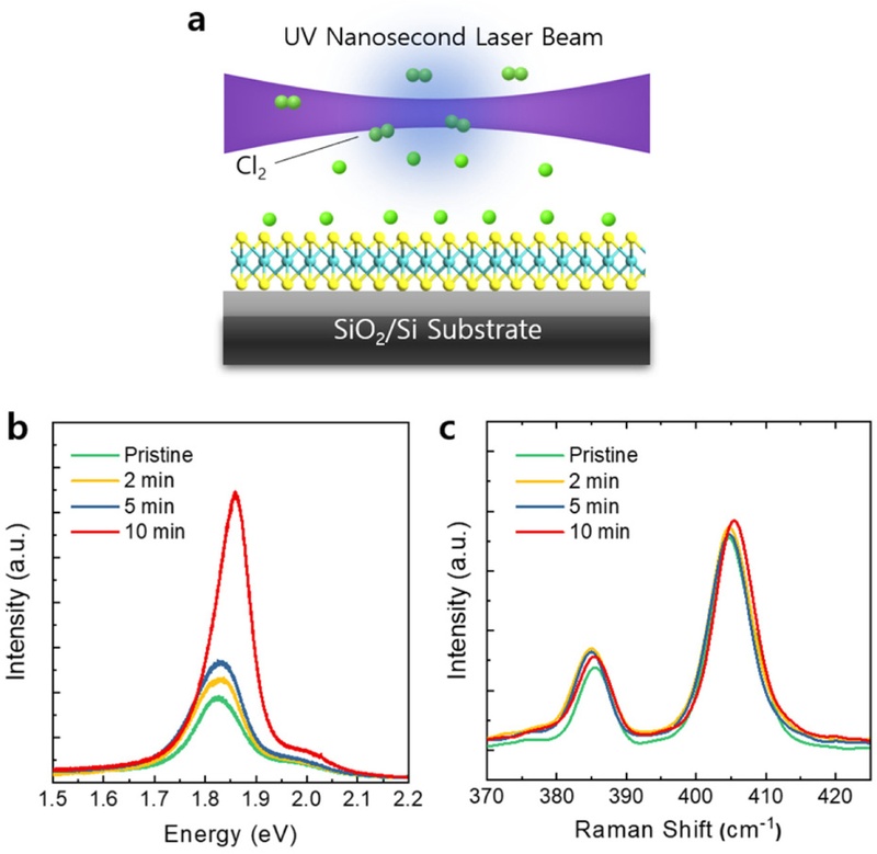
Fig. 1(a) Schematics showing defect generation by normal direction of CW green laser beam on the MoS2 monolayer located on SiO2/Si substrate, (b) PL spectra of MoS2 monolayer in its pristine state and after CW laser irradiation, (c) Temperature distribution of MoS2 monolayer on SiO2/Si substrate obtained by heat transfer simulation, and (d) Normalized lateral temperature distribution of MoS2 monolayer ((T-T0)/(T-T0)MAX) along with the normalized Gaussian laser beam profile (P/PMAX)
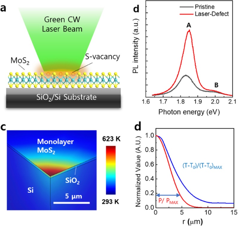
Fig. 2(a) Schematics showing laterally irradiated UV nanosecond laser above MoS2 monolayer on SiO2/Si substrate, showing dissociation of Cl2 molecules and generation of Cl radicals, (b) PL, and (c) Raman spectra of pristine and 2, 5, and 10 min chlorinated monolayer MoS2

We investigated PL and Raman changes upon laser processing using 532 nm excitation laser beam at 0.5 mW and 1800 grating (In-via, Renishaw). For X-ray photoelectron spectroscopy (XPS), PHI 5600 XPS apparatus was used, and CVD-grown monolayer MoS2 was used, as large area sample is needed for XPS analysis.
2.2 Heat Transfer Simulation
The heat transfer simulation was performed using COMSOL Multiphysics software. The thermal boundary conductances (20 between the monolayer MoS
2 (6 Å thickness) and SiO
2 (300 nm thickness), and between the SiO
2 and Si substrate were taken as 20 MW/m
2·K [
8] and 600 MW/m
2·K, respectively. The material properties used in the simulation were as follows: for MoS
2, thermal conductivity of 62.2 W/m·K, density of 5060 kg/m³, and specific heat of 192 J/kg·K; for SiO
2, 1.5 W/m·K, 2650 kg/m³, and 680 J/kg·K; and for Si, 130 W/m·K, 2329 kg/m³, and 700 J/kg·K. The spatial distribution of laser energy absorbed by MoS
2 was modeled as a Gaussian beam profile. Beer-Lambert Law
∂I/∂z=-aSiI was considered for Si region in this simulation. The absorption coefficient of silicon,
aSi at 532 nm is ~ 7.85 × 10
3 cm
-1 and
I denotes laser intensity at location
z. The absorbance of the MoS
2 monolayer on SiO
2/Si substrate was taken as 8% which is calculated based on Fresnel’s equation [
9].
3. Results and Discussion
3.1 Laser-Assisted Defect Generation
The effect of CW laser irradiation on the optical and structural properties of monolayer MoS
2 was investigated using PL spectroscopy. A CW green laser was applied perpendicularly to the surface of mechanically exfoliated MoS
2 on a SiO
2 (300 nm)/Si substrate under vacuum conditions. As shown in
Fig. 1(d), a significant increase in PL intensity was observed in the laser-irradiated region. This enhancement is attributed to the formation of sulfur vacancies caused by local heating. Sulfur vacancies are known to capture atmospheric species, such as N
2, O
2, and H
2O, which attract electrons from MoS
2 and consequently suppress non-radiative exciton decay channels [
10,
11]. Such doping leads to a shift in the excitonic population from negative trions (X-: e-e-h) to neutral excitons (X: e-h), which exhibit stronger radiative recombination. Therefore, the observed increase in PL intensity reflects not only the generation of S-vacancy, but also a modification in the exciton-trion dynamics. These results indicate that CW laser irradiation provides an effective means to locally tune the electronic environment and defect landscape in monolayer MoS
2.
Figs. 1(c) and 1(d) show the temperature profiles of MoS
2/SiO
2 (300 nm)/Si sample obtained by heat transfer simulation under the CW laser illumination. Maximum temperature 623K occurs at MoS
2 layer, which is in the range of the temperature for S-vacancy generation [
11] and well below the thermal sublimation temperature of MoS
2 (800 K) [
12]. Additionally, the lateral temperature distribution of MoS
2 closely follows the Gaussian laser beam profiles with an increased diameter (~16 μm (1/e
2)). Although the MoS
2 monolayer has a lower optical absorbance (8%) than silicon (76%), it reaches a higher peak temperature due to its significantly lower thermal mass (~ρCₚV). This is in contrast to the larger effective thermal volume of silicon, which absorbs the laser over a depth of ~1 μm at 532 nm.
3.2 Laser Assisted Chlorination Process
To induce chlorination, a UV nanosecond pulsed laser beam was introduced in a lateral configuration without touching the pristine monolayer MoS
2. This configuration enables photochemical dissociation of Cl
2 gas molecules, resulting in the generation of chlorine radicals (
Fig. 2(a)). Prior research indicates that Cl atoms can be incorporated directly onto the MoS
2 surface without the need for pre-existing sulfur vacancies, and such treatments (e.g., low-energy Cl
2 plasma exposure) have shown to induce p-type doping behavior [
13]. Furthermore, the Cl radicals generated through photochemical dissociation exhibit low kinetic energy, as confirmed by the absence of plasma-related signatures in the spectral analysis [
14]. This low-energy nature of the dopant species helps to preserve the structural integrity of the MoS
2 monolayer during the doping process.
The laser exposure was conducted for durations of 2, 5, and 10 minutes to investigate the time-dependent effects of doping. As shown in
Fig. 2(b), PL intensity progressively increased with longer processing time. Throughout the process, no noticeable shift or broadening of Raman modes was observed (
Fig. 2(c)), suggesting that the structure of MoS
2 remained unaffected by the treatment.
The observed enhancement in PL intensity and the slight blue-shift of the emission peak can be attributed to chlorine-induced p-type doping: from negative trions (X-: e-e-h) to neutral excitons (X: e-h). This effect arises from chlorine’s high electron affinity, which enables it to capture electrons from MoS
2, thereby reducing electron density and suppressing non-radiative recombination. As a result, excitonic emission is promoted, leading to the observed PL enhancement [
13]. In addition to modulating exciton-trion dynamics, Cl doping alters the electronic band structure of monolayer MoS
2 by lowering the Fermi level through carrier depletion.
X-ray photoelectron spectroscopy (XPS) was employed to examine the chemical composition of MoS
2 after UV-induced chlorination. Prior to doping, CVD-grown pristine monolayer MoS
2 exhibited well-defined Mo 3d and S 2p peaks without any detectable Cl 2p signal, indicating the pristine state of the material (
Fig. 3). Following a 10-minute chlorination process using nanosecond UV laser irradiation, corresponding to the condition that showed the highest PL enhancement in
Fig. 2(b), a prominent Cl 2p peak emerged in the XPS spectrum, confirming the successful incorporation of chlorine species onto the MoS
2 surface.
Fig. 3XPS data obtained from MoS2 monolayer measured before and after chlorination process. (a,b) low resolution spectra, and (c) high resolution spectra near Mo 3d, S 2p, Cl 2p peaks
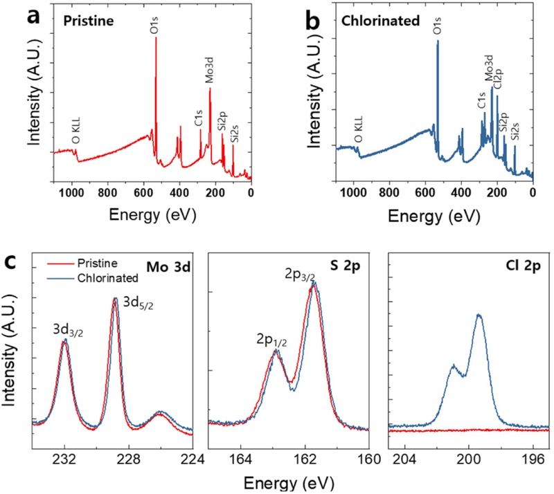
Importantly, no noticeable shifts in the binding energies or intensity ratios of the Mo 3d and S 2p peaks were observed after the doping treatment, suggesting that the overall lattice structure remained intact. The unchanged peak characteristics imply that Cl atoms are physisorbed or weakly chemisorbed onto the MoS
2 surface, without inducing significant structural disruption. This is consistent with the Raman analysis presented in
Fig. 2(c), which similarly showed no evidence of defect formation after chlorination. These findings support that the doping process introduces Cl adatoms in a non-invasive manner while preserving the intrinsic properties of monolayer MoS
2.
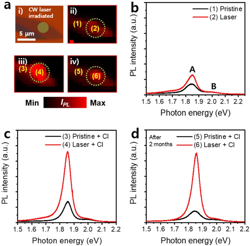
We investigated the synergistic photoluminescence (PL) enhancement in MoS
2 induced by chlorination at laser-generated S-vacancy sites. As shown in
Figs. 4(a) ii and 4(b), S-vacancies were first introduced via CW laser irradiation. These vacancies led to a moderate increase in PL intensity and a slight blue-shifted in the emission peak, likely due to the adsorption of ambient species as discussed in
section 3.1. Subsequently, the CW-laser-treated MoS
2 flakes were transferred to the laser chemical processing system, where a UV nanosecond laser was employed to induce chlorination. After this treatment, regions with pre-existing S-vacancies exhibited a substantially greater PL enhancement compared to pristine areas (
Figs. 4(a) iii and 4(c)). This observation is attributed to the strong binding affinity of Cl atoms at sulfur vacancy sites, reported to be 1.89 eV [
15], which far exceeds the binding energies of typical ambient adsorbates such as N
2 (90 meV), O
2 (110 meV), and H
2O (150 meV), as calculated by density functional theory (DFT) simulation [
13].
Fig. 4(a) i Optical microscope image of MoS2 monolayer on SiO2/Si substrate. PL intensity mapping images and PL spectra obtained from MoS2 monolayer: (a) ii and (b) after CW laser treatment, (a) ii and (c) after subsequent chlorination process, and (a) iv, and (d) after stored in ambient condition for 2 months

Moreover, the vacuum condition applied before chlorination process induces desorption of loosely bound ambient molecules within approximately 15 minutes, as supported by previous in situ PL studies[
10,
11]. Once the vacancies are exposed, Cl radicals readily substitute the desorbed molecules and bind strongly at the defect sites. Importantly, the electron withdrawal per single Cl atom at a S-vacancy site (0.568e) is considerably higher than that on an intact sulfur site of pristine MoS
2 (0.323e) [
13], resulting in a more pronounced p-type doping effect. This defect-assisted doping mechanism leads to a synergistic enhancement of PL in MoS
2.
Furthermore, we observed that the PL intensity remained stable for over two months under ambient conditions in regions with chlorinated sulfur vacancies, whereas the chlorinated pristine areas gradually reverted to their initial PL levels (
Figs. 4(a) iv and 4(d)). This long-term stability is attributed to the significantly higher binding energy of Cl at vacancy sites, approximately 2.5 times greater than that at regular sulfur sites on the pristine surface [
13].
4. Conclusion
We demonstrated localized and stable photoluminescence enhancement in monolayer MoS2 by dual laser beam process, combining a normally irradiated CW laser for sulfur vacancy formation with a laterally coupled UV laser for chlorination process. The selective binding of Cl atoms at S-vacancy sites, supported by previous DFT studies, led to a synergistic p-type doping effect without structural damage. This dual-laser approach enables spatially controlled defect engineering and offers a scalable route for tuning the optical properties of 2D TMDC materials.
REFERENCES
- 1.
Cao, Y., Fatemi, V., Fang, S., Watanabe, K., Taniguchi, T., Kaxiras, E., Jarillo-Herrero, P., (2018), Unconventional superconductivity in magic-angle graphene superlattices, Nature, 556(7699), 43-50.
10.1038/nature26160
- 2.
Wang, Q. H., Kalantar-Zadeh, K., Kis, A., Coleman, J. N., Strano, M. S., (2012), Electronics and optoelectronics of two-dimensional transition metal dichalcogenides, Nature Nanotechnology, 7(11), 699-712.
10.1038/nnano.2012.193
- 3.
Azcatl, A., Qin, X., Prakash, A., Zhang, C., Cheng, L., Wang, Q., Lu, N., Kim, M. J., Kim, J., Cho, K., (2016), Covalent nitrogen doping and compressive strain in MoS2 by remote N2 plasma exposure, Nano Letters, 16(9), 5437-5443.
10.1021/acs.nanolett.6b01853
- 4.
Yang, L., Majumdar, K., Liu, H., Du, Y., Wu, H., Hatzistergos, M., Hung, P., Tieckelmann, R., Tsai, W., Hobbs, C., (2014), Chloride molecular doping technique on 2D materials: Ws2 and MoS2, Nano Letters, 14(11), 6275-6280.
10.1021/nl502603d
- 5.
Biscaras, J., Chen, Z., Paradisi, A., Shukla, A., (2015), Onset of two-dimensional superconductivity in space charge doped few-layer molybdenum disulfide, Nature Communications, 6(1), 8826.
10.1038/ncomms9826
- 6.
Kim, E., Ko, C., Kim, K., Chen, Y., Suh, J., Ryu, S.-G., Wu, K., Meng, X., Suslu, A., Tongay, S., (2016), Site selective doping of ultrathin metal dichalcogenides by laser-assisted reaction, Advanced Materials, 28(2), 341-346.
10.1002/adma.201503945
- 7.
Rho, Y., Lee, K., Wang, L., Ko, C., Chen, Y., Ci, P., Pei, J., Zettl, A., Wu, J., Grigoropoulos, C. P., (2022), A laser-assisted chlorination process for reversible writing of doping patterns in graphene, Nature Electronics, 5(8), 505-510.
10.1038/s41928-022-00801-2
- 8.
Yalon, E., Aslan, B., Smithe, K. K., McClellan, C. J., Suryavanshi, S. V., Xiong, F., Sood, A., Neumann, C. M., Xu, X., Goodson, K. E., (2017), Temperature-dependent thermal boundary conductance of monolayer MoS2 by raman thermometry, ACS Applied Materials & Interfaces, 9(49), 43013-43020.
10.1021/acsami.7b11641
- 9.
Rho, Y., Pei, J., Wang, L., Su, Z., Eliceiri, M., Grigoropoulos, C. P., (2019), Site-selective atomic layer precision thinning of MoS2 via laser-assisted anisotropic chemical etching, ACS Applied Materials & Interfaces, 11(42), 39385-39393.
10.1021/acsami.9b14306
- 10.
Tongay, S., Suh, J., Ataca, C., Fan, W., Luce, A., Kang, J. S., Liu, J., Ko, C., Raghunathanan, R., Zhou, J., (2013), Defects activated photoluminescence in two-dimensional semiconductors: Interplay between bound, charged and free excitons, Scientific Reports, 3(1), 2657.
10.1038/srep02657
- 11.
Tongay, S., Zhou, J., Ataca, C., Liu, J., Kang, J. S., Matthews, T. S., You, L., Li, J., Grossman, J. C., Wu, J., (2013), Broad-range modulation of light emission in two-dimensional semiconductors by molecular physisorption gating, Nano Letters, 13(6), 2831-2836.
10.1021/nl4011172
- 12.
Zhang, Y., Gao, Y., Yao, S., Li, S., Asakura, H., Teramura, K., Wang, H., Ma, D., (2019), Sublimation-induced sulfur vacancies in MoS2 catalyst for one-pot synthesis of secondary amines, ACS Catalysis, 9(9), 7967-7975.
10.1021/acscatal.9b01429
- 13.
Kim, Y., Jhon, Y., Park, J., Kim, C., Lee, S., Jhon, Y., (2016), Plasma functionalization for cyclic transition between neutral and charged excitons in monolayer MoS2, Scientific Reports, 6(1), 21405.
10.1038/srep21405
- 14.
Li, R., Eliceiri, M. H., Li, J., Korakis, V., Yang, R., Rho, Y., Blankenship, B. W., Grigoropoulos, C. P., (2025), Optical emission spectroscopy and gas kinetics of picosecond laser-induced chlorine dissociation for atomic layer etching of silicon, The Journal of Physical Chemistry C, 129(5), 2460-2466.
10.1021/acs.jpcc.4c07330
- 15.
Rastogi, P., Kumar, S., Bhowmick, S., Agarwal, A., Chauhan, Y. S., (2014), Doping strategies for monolayer MoS2 via surface adsorption: A systematic study, The Journal of Physical Chemistry C, 118(51), 30309-30314.
10.1021/jp510662n
Biography
- Yoonsoo Rho
Assistant Professor in the Department of Mechanical Engineering at Ulsan National Institute of Science and Technology. His research interest is the light matter interactions in micro/nano scale and the related science and technologies.