ABSTRACT
Intrinsically stretchable electronics enable seamless integration with dynamic biological tissues and curved surfaces, making them vital for next-generation wearables, biointerfaces, and intelligent robotics. Yet, precise, high-resolution patterning of stretchable electrodes and circuits remains challenging, limiting practical applications. Traditional lithography offers excellent resolution but is hindered by thermal and chemical incompatibilities with soft substrates. Consequently, alternative approaches such as soft lithography, laser-based patterning, printing methods, and electrospray deposition have gained importance. Soft lithography provides an economical, low-temperature option suitable for delicate materials like liquid metals. Laser-based techniques deliver high resolution and design flexibility but require careful parameter tuning for specific substrates. Mask-free printing methods, including direct ink writing and inkjet printing, enable versatile patterning of complex geometries, while electrospray deposition supports precise, non-contact patterning on stretchable surfaces. Collectively, these techniques advance the fabrication of robust stretchable displays, wireless antennas, and bioelectronic interfaces for accurate physiological monitoring. Despite progress, challenges persist, particularly in achieving large-area uniformity, multilayer stability, and sustainable processing. Addressing these issues demands interdisciplinary collaboration across materials science, fluid dynamics, interfacial engineering, and digital manufacturing. This review highlights recent progress and remaining hurdles, offering guidance for future research in stretchable electronics.
-
KEYWORDS: Intrinsically stretchable conductors, Soft electronics, Nano/micro patterning, Materials and architectures, High-resolution patterning
-
KEYWORDS: 본질적 신축성 전도체, 유연전자소자, 나노 마이크로 패터닝, 소재 및 구조, 고해상도 패터닝
1. Introduction
The intricate curvature and repetitive mechanical deformation inherent in human skin, joints, and internal organs present considerable structural and functional barriers to integrating rigid electronic devices directly [
1-
3]. Stretchable electronics offer reliable sensing, signal processing, and data transmission under these conditions. Consequently, they have emerged as essential components in bending. The mechanical durability of these devices is wearable healthcare systems, electronic skin (e-skin), biosignal interfaces, artificial sensory apparatus, and neuromorphic technologies [
4-
7]. Nevertheless, mechanical flexibility alone falls short in enabling advanced applications such as precise monitoring of biological signals, neural stimulation, and bioadaptive computation. Achieving sophisticated mechanical compliance simultaneously with high-density electronic functionality remains a critical goal [
8-
10].
Strategies for achieving mechanical stretchability can be classified into two main categories: structural stretchability and intrinsic stretchability. Structural stretchability designs conventional high-performance inorganic devices or metallic conductors into island-bridge configurations, mesh patterns, or curved geometries, allowing devices to remain undeformed while the surrounding structure absorbs deformation [
11,
12]. While this approach is compatible with established microfabrication methods and generally offers stable performance, practical implementation in multilayer circuits and high-density layouts over prolonged periods introduces significant challenges. Specifically, stress concentrations, gradual fatigue accumulation, and complex packaging issues pose substantial obstacles to effective and durable device integration [
13].
Intrinsic stretchability, on the other hand, employs materials capable of elastic deformation, simplifying device construction by eliminating complex structural arrangements. These materials support monolithic integration, uniform distribution of mechanical stresses, and enhanced long-term reliability [
14,
15]. Achieving effective intrinsically stretchable devices demands balancing inherent stretchability, electrical conductivity, and mechanical integrity. Devices must consistently maintain electrical and mechanical stability through repeated cycles of stretching, compression, and effectively realized through the synergistic integration of optimized structural architectures, robust interfacial adhesion, and continuous conductive pathways which collectively distribute and manage mechanical stresses beyond what is achievable by relying solely on material elasticity [
16,
17].
Contemporary stretchable electronic systems are increasingly designed for comprehensive functionality, integrating densely packed circuits, multifunctional sensing elements, and embedded computational capabilities [
18,
19]. To support these advanced systems, high-resolution patterning technologies with submicrometer precision are essential. Such precision directly affects the integration density, response speed, energy efficiency, and signal quality, thereby significantly influencing the overall device performance [
20,
21].
Despite their advantageous mechanical properties, intrinsically stretchable materials face considerable challenges in preserving structural integrity and precise pattern fidelity during high-resolution fabrication processes [
13,
22]. Patterning these materials involves multiple interacting physical factors, including temperature fluctuations, solvent diffusion, and interfacial stresses, which can lead to pattern distortion, ink dispersion, and structural instabilities [
23,
24]. Consequently, achieving optimal high-resolution patterning demands a thorough understanding of how material properties such as elasticity, viscosity, surface energy, and thermal stability interact under specific processing conditions [
25,
26].
Conductive stretchable materials include carbon-based nanofillers (carbon nanotubes (CNTs), graphene), metal-based nanofillers (silver nanowires (AgNWs), gold nanosheets (AuNSs)), polymer conductors (poly (3,4-ethylenedioxy thiophene) : poly (styrene sulfonate) (PEDOT:PSS)), and liquid metal (Eutectic gallium–indium (EGaIn)). Each material type presents distinct properties influencing pattern transfer efficiency, achievable resolution, processing temperatures, substrate alignment accuracy, and resilience to mechanical stress, even when using identical patterning techniques [
27-
31].
Current high-resolution patterning techniques suitable for intrinsically stretchable materials comprise lithography (photolithography, soft lithography), laser-based methods (laser ablation, laser sintering), and maskless direct-printing techniques (inkjet printing, electrohydrodynamic printing, direct-ink writing, as well as screen, gravure, and offset printing). Each of these methodologies differs significantly regarding compatible materials, achievable minimum pattern size, production speed, and overall productivity [
32-
41]. Effective high-resolution patterning requires precise control over numerous physical interactions, including surface wettability, ink evaporation dynamics, and interfacial stress arising from substrate deformation. Optimal strategies thus systematically address these multi-physical interactions between material properties and specific processing conditions [
42,
43].
Formulating an optimal material-process strategy is critical for designing integrated stretchable electronic devices, ensuring high-density integration, electrical consistency, and prolonged mechanical endurance. This review systematically explores strategies for developing intrinsically stretchable materials, thoroughly summarizes patterning mechanisms, critical process variables, and achievable pattern dimensions, and illustrates practical examples of high-resolution patterning applications. It highlights the potential of integrated material-process methodologies to produce high-performance stretchable electrodes and circuits. Lastly, the review outlines future research directions and identifies key technical challenges requiring attention.
2. Evaluation Metrics for Patterned Intrinsically Stretchable Components
Effective patterning technologies significantly influence the performance and reliability of stretchable electronic applications.
Table 1 summarizes various patterning methods, highlighting their resolutions, advantages, and limitations. Comprehensive evaluation of pattern quality extends beyond the fundamental control of pattern dimensions, necessitating consideration of multiple critical performance metrics. This section details five essential metrics: resolution, electrical performance, mechanical stretchability, optical transparency, and scalability with process compatibility.
Table 1 Typical resolution, advantages, and limitations of patterning methods
Table 1
|
Patterning method |
Typical
resolution [μm] |
Advantages |
Limitations |
Ref. |
|
Photolithography |
5 |
Large-area coverage, ultra-high resolution, industrial mass production |
Expensive equipment, multi-step processes, toxic photoactive compounds, limited to essentially 2D patterning |
[44] |
Nanoimprint lithography
(NIL) |
10 |
Extremely high patterning resolution |
Low throughput, potential damage to delicate nanostructures when removing the mold |
[45,46] |
|
Molding |
10 |
High patterning resolution |
Rough pattern edges |
[46,47] |
Laser
(Direct laser writing) |
10-37 |
High resolution, design flexibility, easily scalable |
Very costly equipment, high energy consumption |
[48,49] |
Substrate modification
patterning |
5-30 |
Enables relatively complex patterns |
Limited to small areas, rough pattern edges |
[50,51] |
Mask-assisted patterning
(Stencil) |
2-10 |
Simple, low cost |
Difficult for complex geometries, lower resolution, edges become rugged when peeling mask |
[52,53] |
|
Inkjet printing |
44-100 |
Non-contact, mask-free, minimal material waste |
Nozzle clogging, reliability issues |
[54,55] |
Electrohydrodynamic
printing (EHD) |
5-20 |
Non-contact, low material waste, relatively high resolution |
Control and reliability issues |
[42,56] |
|
Screen printing |
50-100 |
Adjustable layer thickness, fast deposition |
Screen mesh prone to clogging by nanowire aggregates |
[57,58] |
|
Stamping |
100-150 |
Transferable to curved or non-planar substrates, low cost, stamps can be reused |
Limited resolution (μm scale), stamp wear or deformation over time, requires initial master fabrication |
[27,59] |
Direct ink writing
(DIW) |
20-50 |
Mask-free, non-contact, supports 2D/3D and multi-material structures |
Nozzle resolution limit (tens of μm), relatively slow, requires precise ink viscosity/rheology control |
[32] |
2.1 Resolution: Precision and Minimum Feature Size
Resolution, defined as the smallest achievable feature size, such as line width or pitch, critically impacts circuit integration density and device miniaturization potential [
60]. Advanced applications, including high-resolution displays and dense sensor arrays, typically require resolutions below tens of micrometers. Traditional laser-based techniques and photolithography commonly achieve such precision. Additionally, advanced printing methods such as inkjet and digital printing can also attain high resolution through precise control of nozzle parameters and ink properties.
Electrical performance in patterned electrodes primarily depends on intrinsic material properties, fabrication processes, interfacial adhesion, and connection density [
61]. Typical metrics include sheet resistance (Ω/sq) or volume conductivity (S/cm). Maintaining high electrical conductivity alongside structural integrity and uniformity is essential, particularly in densely integrated circuits where minimal resistance is vital. For printed electrodes, factors such as coating thickness, sintering conditions, and network continuity directly influence electrical performance. Electrical performance is assessed by conductivity retention, with intrinsically stretchable materials required to maintain at least 80% of their initial conductivity under 50% strain [
5,
62].
Mechanical stretchability refers to the capability of an electrode to maintain functional stability during repeated stretching and relaxation cycles [
63]. Mechanical stretchability is categorized as low (reversible tensile strain ≥ 10%), moderate (≥ 50%), and high (≥ 100%) to reflect varying application demands [
62]. This property is evaluated by maximum elongation and electrical stability through cyclic deformation. Applications such as wearable and bio-integrated devices often require stable electrical performance at elongations exceeding 50%. Achieving this performance necessitates strategic structural designs (e.g., 2D-meshes, 3D-wrinkled waves, or controlled-crack configurations) combined with judicious material selection. Practically, electrodes must demonstrate minimal resistance increases (ideally less than approximately 10%) even after thousands of deformation cycles.
Optical transparency, typically quantified by average visible-range transmittance (%), is crucial for applications involving displays, optical sensors, and skin-mounted devices, where minimizing visual obstruction is essential [
77]. Patterns exceeding line widths of approximately 50 µm can be visually intrusive, necessitating finer patterning. Balancing optical transparency and electrical conductivity involves optimizing parameters such as nanowire density, reducing unwanted light scattering, and ensuring smooth surface finishes.
Transitioning from laboratory-scale demonstrations to commercial-scale production demands careful consideration of process repeatability, throughput, equipment compatibility, and efficient material usage [
78]. Achieving uniform pattern quality across large areas (tens of square centimeters or larger) is critical for successful commercialization. Essential factors include maintaining consistent processing speeds, ensuring compatibility between sequential fabrication steps, managing operational temperature ranges, and maintaining chemical stability of inks and photoresists.
3. Correlation Between Material Properties and Compatible Patterning Processes
Conductive materials form the essential basis of stretchable electronic devices, requiring simultaneous fulfillment of critical criteria including electrical properties, mechanical stretchability, process compatibility, and long-term reliability [
17,
79]. To meet these multifaceted requirements, various classes of conductive materials have been developed, each aligning with specific patterning techniques based on intrinsic physicochemical properties. Detailed characteristics of these materials, including electrical performance, stretchability, and compatible patterning methods, are outlined in
Table 2. This section systematically examines major classes of stretchable conductive materials and their associated patterning methods.
Table 2 Conductive materials for stretchable electronics
Table 2
|
Materials |
Electrical performance |
Stretchability [%] |
Process |
Ref. |
|
Carbon filler |
2,200 S/m / 7 Ω/sq-1.8kΩ/sq. |
60-200 |
Mask, Laser, Stamp, Screen Printing, Nozzle Printing |
[27,64-67] |
|
Metal filler |
6 × 10⁴ S/m - 8 × 10⁵ S/m /
0.24 Ω/sq-21 Ω/sq |
50-900 |
Photolithography, Lift-off, Nozzle printing, Inkjet printing,
Screen printing, Mold |
[28,29,68-70] |
|
Liquid metal |
1.3 × 10⁶ S/m |
130-1,000 |
Photolithography, Blade Coating, laser, Nozzle printing |
[30,50,71-73] |
|
Conductive polymer |
10-4,100 S/m |
100-500 |
Photolithography |
[31,74-76] |
3.1 Carbon-based Conductive Materials
Carbon-based conductive materials, such as CNTs, graphene, and carbon black, are extensively utilized due to exceptional mechanical flexibility and relatively low sheet resistances (7 Ω/sq to 1.8 kΩ/sq) [
27,
66,
67]. Particularly, CNTs form highly conductive percolation networks through their high aspect ratios, ensuring stable electrical performance during mechanical deformation like stretching and bending [
64,
67]. With advantageous particle size distribution and dispersibility, these materials are well-suited to printing techniques including screen printing, nozzle printing, mask-assisted deposition, stamp transfer, and laser-based patterning. Furthermore, their low-temperature and large-area processing compatibility facilitate efficient commercial-scale manufacturing, combining stretchability with production practicality.
Metallic nanomaterials—including AgNW, gold nanowire (AuNW), AuNS, and nanoparticles of gold (AuNPs) and copper (CuNPs)—exhibit high conductivity ranging from 6 × 10⁴ S/m to 8 × 10⁵ S/m, and sheet resistances between 0.24 Ω/sq and 21 Ω/sq, suitable for advanced electronics [
28,
29,
68,
70]. These materials uniquely merge superior electrical conductivity with exceptional stretchability (50%-900%), addressing demanding application criteria [
69,
70]. Patterning methods such as photolithography, lift-off processes, nozzle printing, inkjet printing, and mold-based fabrication are particularly effective. AgNWs notably offer excellent thermal and optical stability, enabling precise patterns through photolithography and nozzle printing techniques, supporting high-resolution circuits requiring rapid signal processing.
Gallium-based liquid metals, particularly EGaIn, provide intrinsically stretchable conductivity (1.3 × 10
6 S/m) and outstanding mechanical elongation capability (130%-1,000%) [
50,
71]. Their inherent fluidity accommodates complex mechanical deformations—including stretching, compression, and bending—without sacrificing electrical performance [
30,
72]. These materials are compatible with various processes such as photolithography, blade coating, laser cutting, and nozzle printing. Precision patterning is achievable by manipulating surface tension and oxide layers. Moreover, techniques involving microchannel fabrication and microstructured injection enable precise circuitry formation on complex, curved, or three-dimensional surfaces.
Conductive polymer materials such as PEDOT:PSS and polyaniline feature conductivities from 10 S/cm to 4,100 S/cm [
31,
74]. Despite lower conductivity relative to metals, these polymers provide reliable mechanical stretchability (50%-100%), superior solution processability, substrate adhesion, transparency, and mechanical flexibility, advantageous for biointerface and wearable applications [
75,
76]. Conductive polymers demonstrate compatibility with photolithographic methods, where photoresponsive additives or polymers enable direct pattern formation without additional etching. Solution-based methods such as spin coating and inkjet printing allow for uniform thin-film deposition suitable for high-resolution electrodes and large-area applications.
Each class of conductive material offers distinctive electrical, mechanical, and process compatibility characteristics optimized for specific applications. Carbon-based materials are particularly suitable for printing processes, metallic nanomaterials provide precise and scalable patterning, liquid metals excel in complex architectures, and conductive polymers offer versatile processing for biocompatible interfaces. Comprehensive details on these materials and their patterning techniques are provided in
Table 3. Thus, the integrated consideration of material-specific characteristics and suitable patterning methodologies remains a fundamental strategy for advancing the performance and scalability of future stretchable electronic systems.
Table 3Overview of recent advancements in stretchable electrodes
Table 3
|
Filler |
Matrix |
Patterning method |
Resolution
[μm] |
Electrical
properties |
Stretchability
[%] |
Durability |
Application |
Ref. |
P3-SWNT
CNT |
SEBS |
Lift-off |
2 |
ΔR/R₀ < 1.5 @ 100% |
100 |
1,000 cycles
@ 25% |
Organic transistor arrays |
[80] |
|
CNT |
SEBS |
Lift-off |
1 |
727.2 Ω/sq |
100 |
1,000 cycles
@ 100% |
Tactile sensor array,
LED display |
[18] |
AgNP &
MWCNT |
PDMS |
DIW |
150 |
ΔR/R₀ <10 @ 10% |
74 |
1,000 cycles |
Strain sensor |
[81] |
CB/
MWCNT |
TPU |
Screen printing |
50 |
R < 300 KΩ |
50 |
300 cycles
@ 10% |
Strain sensors |
[82] |
|
CNT |
Ecoflex |
Stamp |
150 |
~1.8 kΩ/sq |
200 |
5,000 cycles
@ 85% |
Strain sensing |
[27] |
|
GO |
PDMS |
DIW |
50 |
1.61 kΩ·cm, ΔR <
1,100 @ 40% |
40 |
1,000 cycles
@ 20% |
Strain sensors |
[83] |
|
AgNW |
PDMS |
Screen printing |
50 |
1.9 Ω/sq @
52% transmittance |
100 |
|
Circuit boards |
[57] |
|
AgNW |
VHB |
DIW |
50 |
1.26 × 10⁵ S/cm |
90 |
1,000 cycles
@ 50% |
Soft electro adhesion
grippers |
[84] |
|
AgNW |
SEBS |
Mask Pattern |
100 |
10 Ω/sq @ 50% |
100 |
1,000 cycles
@ 20% |
Diodes, O-gain antenna, etc. |
[85] |
|
AgNW |
PDMS |
Electrospray
deposition |
~50 |
2.7 Ω/sq @ 43.6%
transmittance |
12 |
|
Triboelectric tactile sensor
array, driving LED map
upon touch |
[86] |
|
AgFD |
textile |
Screen printing |
100 |
0.088 Ω sq⁻¹ |
154 |
1,000 cycles
@ 100% |
Strain sensors |
[87] |
|
AuHNW |
SEBS |
Photolithography |
50 |
2.65 Ω/sq |
100 |
1,000 cycles |
@ 50% |
Integrated patch combining
strain sensor, temperature
sensor, etc. |
[88] |
|
AuNW |
PDMS |
Masked Pattern |
100 |
50 Ω |
50 |
|
Porcine sciatic nerve
stimulation cuff |
[89] |
EGaIn-
AgNW |
Freestanidng |
Laser |
100 |
5.79×10⁵ S/m |
1,350 |
10,000 cycles
@ 100% |
Stretchable circuit |
[90] |
|
EGaIn @ Cu |
VHB tape |
Laser |
5 |
4.08 × 10⁴ S/cm @
0% strain |
600 |
1,000 cycles
@ 200% |
Luminous wristband, strain
sensor, visible thermal
therapy panel |
[91] |
|
bGaIn |
PDMS, VHB |
Mask Pattern |
25 |
R/R₀ ≈ 1.06 @
100% on PDMS |
1,000 |
1,500 cycles
@ 100% |
Circuit board assemblies
(strain circuits, LED
displays, and capacitive
sensing) |
[92] |
|
CNT/LM |
PDMS |
3D Printing |
5 |
ΔR/R₀ = 4 @
100% |
100 |
10,000 cycles
@ 100% |
3D electrical interconnects |
[93] |
|
EGaIn |
PEGDA
hydrogel |
Stamp |
100 |
ΔR/R₀ = 2.3 @
1,500% |
1,500 |
1,400 cycles
@ 700% |
Strain sensor, Stretchable
LED Digital circuit |
[59] |
|
EGaIn |
SiS |
Litho-graphy |
20 |
3 × 10⁶ S/m |
2,500 |
1,500 cycles
@ 100 % |
Displays, strain sensors,
Joule heaters, Humidity/
breath sensors, etc |
[94] |
|
EGaIn |
SBS |
μLME
patterning |
2 |
ΔR/R₀ ≈ 0.6% @
300 % |
1,500 |
100 cycles
@ 1000 % |
Implantable neural interface
(ECoG) arrays |
[95] |
|
EGaIn |
TPU |
DIW |
10 |
ΔR/R₀ ≈ 0% @
300% strain |
460 |
2,000 cycles
@ 60% |
Wideband stretchable
antenna |
[32] |
|
Ag-GaIn |
SIS |
DIW |
140 |
7.02 × 10⁵ S/m |
600 |
1,000 cycles
@ 30% |
NFC tags, LED matrices,
strain gauges, RFID antennas |
[96] |
|
PEDOT: PSS |
SEBS |
Inkjet printing |
500 |
ΔR/R₀ = 1.49 @
55% |
55 |
200 cycles
@ 55% |
Transparent electrodes |
[97] |
|
PEDOT: PSS |
SEBS |
Photo patterning |
20 |
1,000 S/m |
40 |
1,000 cycles
@ 30% |
Transparent capacitive touch
sensors, EOG, ECG, EMG
biosensors |
[98] |
4. Subtractive Patterning Methods for Intrinsically Stretchable Electronics
Subtractive patterning methods involve selectively removing regions from a uniformly deposited conductive film or network, leaving the targeted circuit geometry intact [
99-
101]. This approach is widely adopted for applications requiring high resolution and precise feature definition, and it is applicable to various conductive materials including metallic nanowires, conductive polymers, and liquid metals [
73,
99]. This section comprehensively discusses subtractive techniques, highlighting lithography-based and laser-based patterning methods and their implementations.
Lithography processes deliver high-resolution patterns with consistent reproducibility, extensively validated in semiconductor manufacturing. Lithographic techniques generally comprise photolithography and soft lithography, each with distinct characteristics regarding resolution, cost-effectiveness, and process complexity.
4.1.1 Photolithography
Photolithography employs ultraviolet (UV) exposure and a photoresist (PR) to precisely define conductive patterns, followed by an etching step that removes non-desired regions [
102,
103]. This foundational technique is essential for stretchable electronics, as it enables high-resolution, reproducible patterns necessary for reliable device functionality. Achieving optimal performance in stretchable applications particularly requires careful compatibility and chemical stability among the PR, substrate, and conductive materials, alongside meticulous control of process parameters to minimize deformation-related distortions [
104-
106]. This technique necessitates compatibility between the PR, substrate, and conductive materials, as well as chemical stability during the etching process. Careful selection of process parameters is crucial to minimize distortions due to substrate deformation, particularly in stretchable device applications.
Highlighting the necessity for environmentally sustainable and simplified processing, Yoo et al. developed solvent-free photolithography for patterning AgNW using UV-curable pressure-sensitive adhesive (PSA). This approach effectively balances resolution (down to 8 µm), process efficiency, and eco-friendliness, making it highly suitable for applications such as transparent heaters and electrowetting-on-dielectric devices [
44].
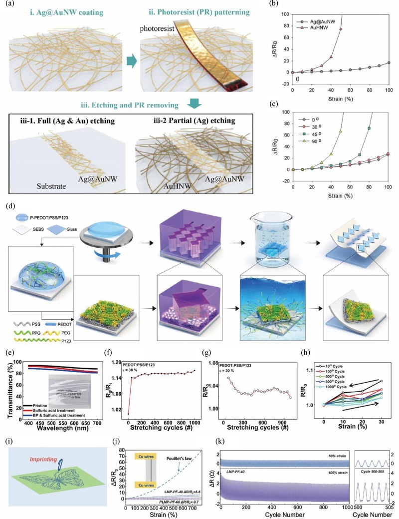
To address mechanical reliability and electrical performance under significant strain, Kim et al. introduced selective photolithography-based etching for silver-gold core-shell nanowires (Ag@AuNWs) and hollow gold nanowires (AuHNWs). The resulting patterns achieved approximately 50 µm resolution and demonstrated stable electrical performance, emphasizing their practical viability for flexible circuits and sensors (
Figs. 1(a)-1(c)) [
88].
Fig. 1(a)-(c) Schematics illustrating two distinct etching techniques for monolithic pattern fabrication and resultant patterns demonstrating angular variations [88], (d) Illustration of the photopatterning process for PEDOT:PSS, highlighting that areas exposed to UV become water-soluble within 10 seconds, (e) Optical transmittance characteristics of PEDOT:PSS films on SEBS substrates across the visible wavelength range, (f) Normalized resistance change at 0% strain (R₀) across repeated stretching cycles, referenced to initial resistance (Rᵢ) before cyclic deformation, (g) and (h) Normalized resistance changes under cyclic 30% strain conditions, demonstrating hysteresis effects during repeated mechanical cycling [98], (i) Schematic representation of conductive pathway formation on LM-PFs surfaces through imprint lithography, (j) Comparative analysis of resistance trends for LMP-PF-40 and PLMP-PF-60 composites with applied strain, theoretical resistance variations based on Pouillet’s law, and schematic of the experimental sample (inset), and (k) Resistance variations of LMP-PF-40 composite under repeated 50% and 100% stretching cycles over 1,000 cycles [107]. To enhance visual clarity, limited font size adjustments were made in select panels while preserving the integrity of the original figures (Adapted from Refs. 88,107 with permission and Ref. 98 on the basis of OA)

Recognizing the challenges associated with traditional lithographic methods for organic conductors, Yoon et al. introduced a water-based photolithography technique tailored for poly (3,4-ethylenedioxythiophene) : poly (styrene sulfonate) (PEDOT:PSS). This method leveraged UV-induced changes in hydrophilicity to selectively dissolve unexposed regions, enabling stable, high-resolution (~25 µm) patterning, high optical transparency, and robust electrical integrity during repeated mechanical cycling (
Figs. 1(d)-1(h)) [
98].
To further expand applicability to extreme mechanical conditions, Wu et al. developed digital light processing (DLP)-based projection lithography for EGaIn liquid metal patterning. Through rapid UV exposure and mechanical sintering, this approach achieved highly conductive patterns (~20 µm resolution) that maintained electrical performance under strains exceeding 2,500%, underscoring their suitability for demanding stretchable device applications (
Figs. 1(a)-1(d)) [
94].
4.1.2 Soft Lithography
Soft lithography employs elastomeric molds, primarily polydimethylsiloxane (PDMS), to transfer or form conductive patterns onto substrates under low-temperature and low-pressure conditions [
108,
109]. This approach is particularly valuable for stretchable electronics due to its compatibility with sensitive substrates and its ability to produce complex patterns without high-cost infrastructure. Various methods, including microcontact printing, imprint lithography, replica molding, and microtransfer molding, allow tailoring processes to specific application needs. Effective implementation necessitates careful management of mold structural integrity, ink viscosity, and precise substrate-mold interactions [
38,
110]. It encompasses methods such as microcontact printing, imprint lithography, replica molding, and microtransfer molding, each tailored for specific processing needs. Key considerations include mold structural integrity, ink viscosity, and substrate-mold interaction [
110-
112]. In addressing the need for reproducible high-resolution patterning coupled with mechanical robustness, Chen et al. utilized imprint lithography to pattern liquid metal polymer (LMP) composites. This method produced consistent patterns demonstrating exceptional mechanical compliance and electrical stability under considerable deformation, highlighting its applicability in advanced flexible electronics (
Figs. 1(i)-1(k)) [
107].
Further emphasizing the capability of soft lithography for ultrafine resolution and scalable manufacturing, Zhuang et al. demonstrated wafer-scale soft lithography to produce ultrahigh-resolution liquid metal electrodes (~2 µm feature size). These electrodes provided stable electrical performance even under extensive mechanical strain, supporting their potential integration into biointegrated electronics and other demanding stretchable device applications [
95].
Laser-based patterning represents a significant advancement in stretchable electronics, enabling rapid, precise, and noncontact fabrication of high-resolution electrode patterns without the limitations of physical masks. Techniques such as laser ablation, selective retention via laser-induced adhesion, and laser-induced graphene (LIG) each offer distinct benefits tailored to specific requirements within the field.
4.2.1 Laser Ablation
Laser ablation involves selectively removing conductive materials through high-energy laser exposure. Precise control of laser parameters, including wavelength, pulse duration, and scan speed, ensures minimal thermal impact on substrates and surrounding materials, achieving high pattern resolution crucial for device performance.
As a representative case highlighting this method's capability for high-resolution and flexible electronics, Zhang et al. employed femtosecond laser ablation to pattern liquid metal-copper composites, attaining precise patterns down to 5 µm resolution. This approach demonstrated robust electrical stability under diverse mechanical strains, positioning it as a key strategy for fabricating high-performance wearable and flexible circuits (
Figs. 2(f)-2(i)) [
113].
Fig. 2(a)-(e) Schematic depicting the fabrication process for LM@Cu patterned electrodes, (f) LM@Cu electrodes under twisting, bending, and stretching deformation conditions, (g) Variation of normalized resistance (R/R₀) of LM@Cu electrodes as a function of twisting angle, (h) R/R₀ changes under outward and inward bending conditions, (i) Relative resistance change (ΔR/R₀) for LM@Cu electrodes under stretching from 0% to 600% [91], (f) Fabrication schematic for FS-GaIn circuits, (g) Electromechanical characterization comparing pristine and repaired FS-GaIn circuits, (h) Relative resistance change under uniaxial stretching at 0.5 mm s-1 for FS-GaIn integrated with a zero-ohm resistor (inset: digital image of the resistor-integrated FS-GaIn circuit) [90], (i) Complete fabrication workflow illustrating LIG patterning on both substrate sides, via and tab formation, tab removal post-copper plating, solder paste application, and assembly of surface-mount components, (j) Relationship between sensing element resistance and applied strains ranging from 5% to 25%, and (k) Sensor resistance stability across ten repeated stretching cycles at varying strains [114]. To improve readability, font sizes were carefully adjusted in some panels, with the original figure content maintained without alteration (Adapted from Ref. 91 with permission and Refs. 90,114 on the basis of OA)
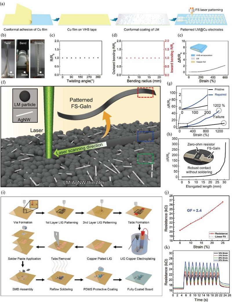
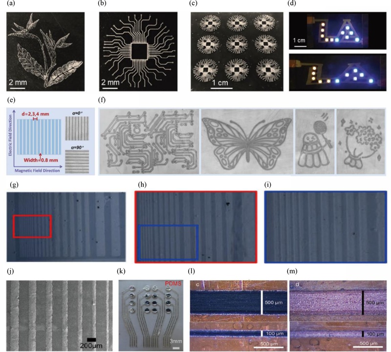
Fig. 3(a)-(c) Printed LM patterns demonstrating a Strelitzia reginae flower, circuit designs, and circuit arrays [94], (d) Stretchable LM circuit integrated on an SIS substrate connected to LEDs, (e) Schematic and optical images depicting the imprinting strips used in electromagnetic interference shielding effectiveness (EMI SE) testing, where angle α denotes stripe-electric field orientation, (f) Representative printed LM patterns illustrating circuits, butterfly, shuttlecock, and flower designs [107], (g)-(i) Stereomicroscopic images of patterned PEDOT:PSS films, scale bars correspond to 1,000, 500 and 200 µm respectively [98], (j) SEM images depicting a series of optimized laser-induced streak patterns [91], (i) Optical images illustrating LIG traces on polyimide substrates before and (m) after copper plating, with line widths ranging from 50 µm to 2 mm [114] (Adapted from Refs. 91,94,98 with permission and Refs. 98,114 on the basis of OA)
4.2.2 Selective Retention via Laser-induced Adhesion
Selective retention through laser-induced adhesion capitalizes on localized interfacial chemical reactions or adhesion enhancements induced by precise laser irradiation. This method uniquely enables maskless, highly accurate patterning while ensuring strong mechanical adhesion critical for sustained electrode performance under extreme deformation.
To underscore this method’s potential, Kim et al. developed a liquid metal-silver nanowire composite electrode patterned using femtosecond laser multiphase sintering and selective etching. The resulting freestanding electrodes exhibited extraordinary mechanical performance, including stretchability exceeding 1,350% and long-term durability through over 10,000 deformation cycles. These characteristics notably support advanced applications such as conformal electronics and self-healing devices (
Figs. 2(a) and 2(b),
3(a) and 3(b),
4(a) and 4(b)) [
90].
4.2.3 Laser-induced Graphene
LIG directly transforms polymer substrates into conductive graphene patterns via laser-driven carbonization. This technique significantly reduces material usage and simplifies processing steps, enhancing the overall sustainability and efficiency of electrode fabrication.
Demonstrating the efficacy of this method for complex circuit architectures, Babatain et al. successfully fabricated dual-sided circuit boards employing LIG on polyimide substrates. These electrodes, featuring high-resolution patterns (~100 µm) and maintaining stable electrical performance under strain, are ideally suited for sophisticated wearable electronics and sensing applications (
Figs. 2(j) and 2(k),
3(l) and 3(m)) [
114].
In summary, laser-based subtractive patterning techniques provide pivotal solutions for creating advanced stretchable electronics, offering substantial flexibility in design and application. These methods are essential to achieving precise control over electrode geometry, mechanical reliability, and functional performance. Future developments will likely explore hybrid integration approaches, combining laser patterning techniques with novel materials and complex substrate architectures to expand their applicability further.
5. Large-area Parallel patterning Methods for Intrinsically Stretchable Electronics
Conventional photolithography and precision deposition-based patterning techniques achieve high resolution down to the tens-of-nanometer scale but typically require cleanroom facilities, multiple mask alignments, and intricate operational procedures, restricting their widespread use in compliant stretchable electronics. Consequently, solution-based additive patterning methods, characterized by operational simplicity and compatibility with diverse materials and flexible substrates, have become essential alternatives. This section provides a comprehensive overview of substrate modification, mask-assisted patterning, and various printing-based methods, underscoring their significance in manufacturing stretchable electronic devices [
33,
117-
120].
Substrate modification selectively localizes conductive inks without traditional masking or complex lithographic processes. Approaches based on substrate wettability and microstructured surfaces precisely control ink deposition and enhance adhesion, greatly improving device performance under mechanical stress [
46,
121,
122].
5.1.1 Wettability-controlled Patterning
Wettability-controlled patterning involves selectively modifying substrate surfaces to exhibit distinct hydrophilic and hydrophobic regions, effectively directing conductive inks without chemical or mechanical interference [
123,
124]. Ma et al. demonstrated precise ink deposition using thermally adhered parafilm masks, selectively forming hydrophilic areas, achieving high-resolution AgNW patterns on stretchable substrates such as styrene ethylene/butylene styrene (SEBS) and PDMS, crucial for transparent and stretchable electrodes [
125]. Zhu et al. developed a vapor-phase polymer coating technique combined with oxygen plasma, allowing maskless patterning compatible with various substrates and complex geometries [
122]. These studies highlight the practicality and flexibility of wettability-controlled patterning for large-area and bio-integrated stretchable electronics.
5.1.2 Surface Microstructure-based Patterning
Surface microstructure-based patterning uses micro- and nanoscale topographical features to control conductive ink deposition and enhance mechanical integrity [
46,
118]. Guo et al. demonstrated high-resolution electrode fabrication using microstructured substrates, precisely modulating multiwalled carbon nanotube and graphene ink deposition (
Fig. 4(a)) [
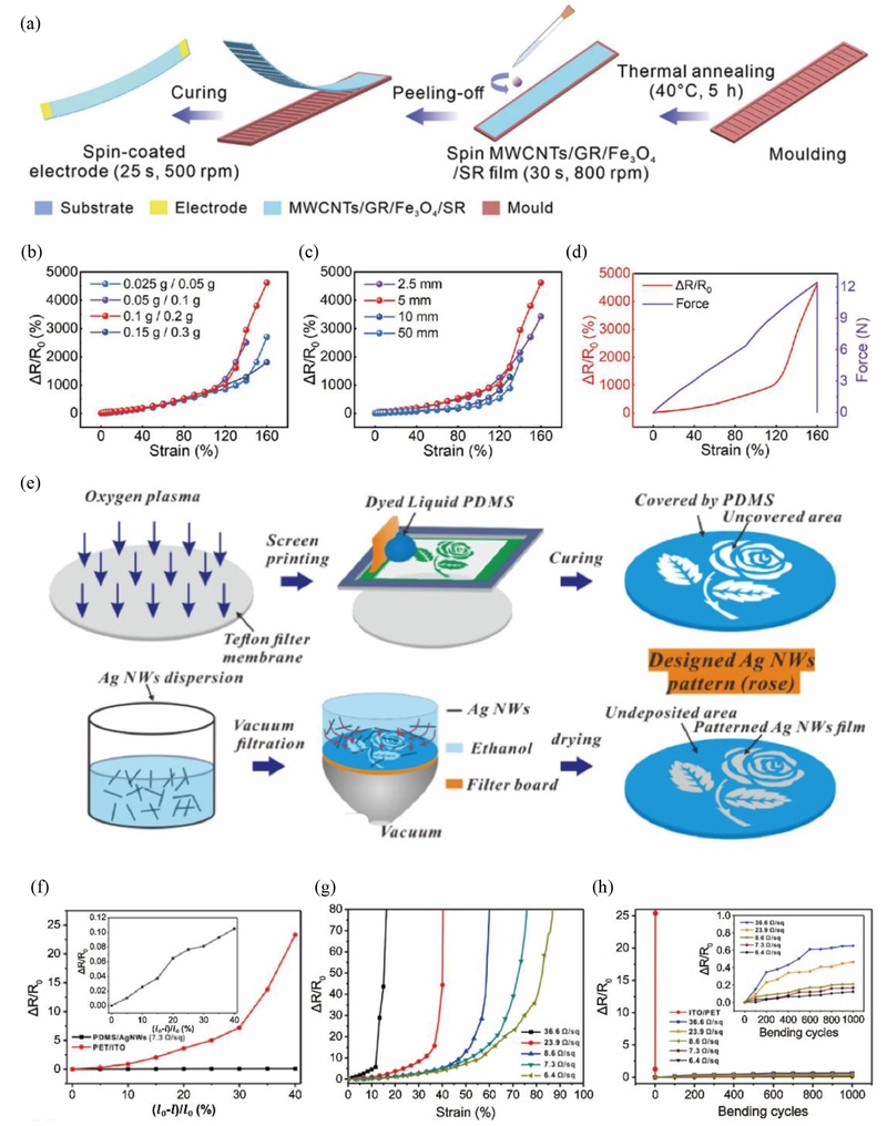
115]. This approach notably improved device sensitivity and mechanical robustness under extreme stretching (
Figs. 4(b)-4(d)). Vu et al. and Yang et al. further illustrated that integrating porous microstructures into substrates simultaneously improved mechanical stretchability, gas permeability, and precise ink deposition, underlining the multifunctionality imparted by structured patterning in stretchable sensor platforms (
Figs. 6(a)-6(d)) [
126,
127].
Fig. 4(a) Schematic of bioinspired sensing layer architecture, (b) Strain-dependent response of DMSSS sensing layers incorporating varying masses of MWCNTs/GR, (c) Relationship between microstructure spacing ratio and applied strain for DMSSS sensing layers, (d) Relative resistance changes in DMSSS during tensile failure testing [115], (e) Schematic of the AgNW patterning process, (f) Resistance variations of AgNW/PDMS transparent conductive films (TCF) and commercial ITO/PET electrodes under different compression ratios, (g) Resistance response of AgNW/PDMS TCFs with varying sheet resistances from 0% to 100% strain, and (h) Cyclic resistance stability for AgNW/PDMS TCFs and commercial ITO/PET electrodes at 40% compression strain [116]. To enhance visual clarity, limited font size adjustments were made in select panels while preserving the integrity of the original figures (Adapted from Refs. 115,116 with permission)
5.2 Mask-assisted Patterning
Mask-assisted methods use predefined masks to selectively deposit conductive inks, eliminating the need for high-temperature or vacuum environments [
53,
128]. Lin et al. effectively utilized patterned PDMS masks combined with rolling pressure to achieve high-resolution AgNW electrodes with minimal resistance variation during mechanical cycling (
Figs. 4(e)-4(h),
6(e)-6(h)) [
116]. Similarly, Wang et al. employed laser-patterned masks to fabricate multilayer liquid metal electrodes on electrospun TPU substrates, demonstrating the efficacy of this technique in creating highly patterned and stretchable electronic circuits with accurate alignment and superior mechanical resilience (
Figs. 5(a)-5(d)) [
129].
Fig. 5(a) Structural schematic of bioinspired sensing layer, (b) and (c) Uniaxial tensile stress-strain curves in transverse (T) and longitudinal (L) directions for membranes prepared at different rotational speeds: TPU (b) and TPU/LM (c), (d) Cyclic tensile stress-strain behavior of TPU/LM wires at 100 rpm under 50% transverse strain [129], (e) Schematic illustrating deformable, self-healing EGaIn electrodes on hydrogels, (f) Resistance variation under strain for a series of hydrogels investigated, (g) Comparative analysis of resistance change ratios against previously reported stretchable conductors [59], (h) Scalable printing process schematic with water-spray sintering, (i) Resistance stability across increasing cyclic strain, and (j) Resistance versus strain until failure for varying printed line widths [136]. To improve readability, font sizes were carefully adjusted in some panels, with the original figure content maintained without alteration (Adapted from Refs. 59,129 with permission and Ref. 136 on the basis of OA)
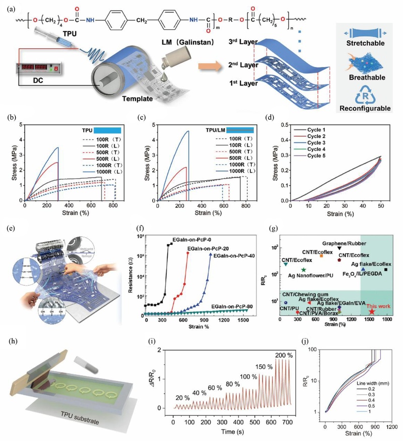
Fig. 6(a) Optical photograph of patterned PPDL on ITO/PET substrate, (b)-(d) SEM images showing top view (b) and (c), and cross-sectional view (d) of the PPDL [126], (e) Microscopic images of patterned AgNW electrodes with different linewidths, (f) and (g) Photographs demonstrating various complex shapes formed by AgNW patterns; scale bar = 5 mm, (h) Transparent conductive AgNW/PDMS film patterned into a rose shape on semi-cured PDMS; scale bar = 10 mm [116], (i) Transferred micropatterned EGaIn electrodes onto hydrogels, (j) Photographs of micropatterned high-density EGaIn electrodes under lateral stretching, (k) Optical microscopy of periodic 100 µm-wide EGaIn lines [59], (l) Screen-printed liquid metal patterns on stretchable TPU substrates; scale bar = 5 cm, and (m)-(o) Demonstration of mechanical robustness of printed NFC circuits under realistic deformations including stretching (m), twisting (n), and successful smartphone reading when mounted on textile substrates (o) [136] (Adapted from Refs. 59,116,126 with permission and Ref. 136 on the basis of OA)

5.3 Transfer Printing
Transfer printing involves depositing conductive materials onto intermediate carriers and subsequently transferring these patterns onto target substrates, enabling precise patterning of materials challenging to print directly [
130,
131]. Park et al. successfully demonstrated transfer printing of EGaIn liquid metal onto porous substrates, achieving outstanding electrical stability under strains exceeding 1,500% (
Figs. 5(e)-(h),
6(i)-6(k)) [
59]. Liang et al. and Yang et al. further enhanced this method by employing microstructured stamps and capillary-driven self-assembly, enabling precise control over filler orientation, alignment, and density [
27,
132]. Thus, transfer printing has emerged as an indispensable technique for integrating complex conductive materials into precisely structured stretchable electronic devices.
Screen printing accurately deposits high-viscosity conductive inks through patterned screens onto substrates, making it particularly suitable for stretchable electronics that demand stable electrode performance under repeated mechanical deformation [
133-
135]. Shang et al. successfully demonstrated screen-printed liquid metal patterns, creating microstructured circuits with stable electrical performance under significant strain (
Figs. 5(h)-5(j),
6(l)-6(o)) [
136]. The ability to form uniform, high-resolution patterns and robust electrode structures confirms screen printing as a key method for scalable production of stretchable electronics, particularly in wearable applications.
Gravure printing is recognized for high-speed, high-resolution patterning, ideally suited for large-scale, continuous manufacturing processes required in multilayer stretchable electronics [
137-
139]. Kawakami et al. effectively utilized gravure printing to fabricate layered stretchable circuits featuring vertical interconnections, maintaining precise alignment and reliable performance under mechanical strain [
140]. The scalability and compatibility of gravure printing with multilayer structures underscore its potential for industrial-scale production of advanced stretchable electronic devices.
Reverse offset printing employs an indirect transfer process, enabling high-resolution patterning with minimal ink bleed, well-suited for intricate multilayer electrode designs [
141,
142]. Kim et al. demonstrated the capability of reverse offset printing to create double-layered AgNW transparent electrodes, precisely controlling pattern alignment and surface uniformity, essential for high-density, multilayer device architectures [
143]. The adaptability of reverse offset printing to high-viscosity inks validates its effectiveness for sophisticated stretchable electronic applications.
Collectively, these additive patterning methodologies present robust solutions to the challenges inherent in manufacturing stretchable electronics, providing flexibility in design, scalability in production, and compatibility with diverse materials and substrates. Further integration of these methods with novel materials and structural architectures is expected to significantly advance the innovation and adoption of stretchable electronic technologies.
6. Serial Direct Printing Patterning Techniques for Intrinsically Stretchable Electronics
Printing-based patterning methods directly deposit conductive inks onto designated regions, forming electrode patterns without complex lithographic or mask-based processes [
55,
144]. These techniques are valued for their simplicity, low manufacturing costs, and compatibility with diverse substrates, making them highly attractive for stretchable and wearable electronic applications. This section details representative printing techniques, including direct ink writing (DIW), inkjet printing, and electrospray deposition, emphasizing their relevance and effectiveness in the field of flexible electronics.
DIW involves extruding highly viscous conductive inks through a fine nozzle directly onto substrates, enabling precise patterning without masks [
32,
148]. Optimal DIW inks exhibit shear-thinning behavior, ensuring high fluidity during extrusion and rapid viscosity recovery post-deposition to preserve structural integrity. Conductive materials frequently [
149,
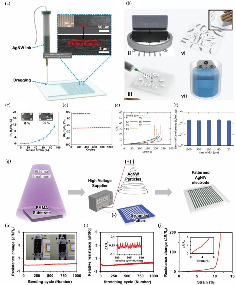
150]. used include AgNWs, graphene oxide (GO), CNTs, and liquid metal composites. Kong et al. demonstrated high-resolution DIW using AgNW inks stabilized with sodium alginate, achieving stable patterns with resolutions down to 50 µm across various substrates (
Figs. 7(a) and
8(a)-8(b)) [
84]. Post-treatment improved conductivity and mechanical reliability significantly, making the method suitable for versatile and robust stretchable electrodes (
Figs. 7(c) and 7(d)). Shi et al. developed an EGO-PDMS [
83]. Min et al. utilized an aerodynamically focused nanomaterials system to print AgNP/MWCNT composites, resulting in sensors with exceptional gauge factors and stretchability [
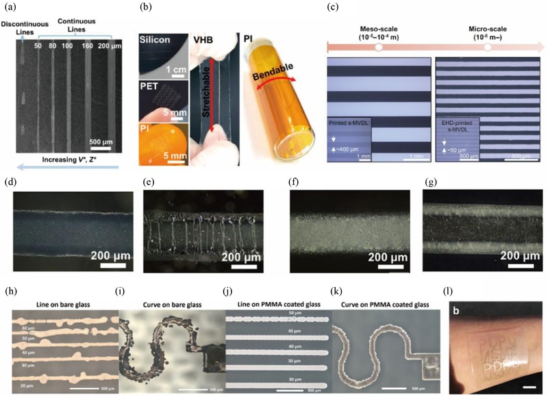
81]. Nanocomposite ink, achieving sensitive strain sensors with a linear response and high durability under repeated stretching. Jeong et al. advanced DIW using a metal-vapor-desorption layer (MVDL) technique, enabling fine, maskless metal patterning with line widths below 8 µm on complex substrates (
Fig. 8(c)) [
146]. These examples illustrate DIW’s unique combination of high resolution, material versatility, and compatibility with curved, stretchable substrates.
Fig. 7(a) Schematic diagram of the direct writing process [84], (b) Sequential schematic illustration of conductive track fabrication, beginning with PVA spin coating, followed by inkjet printing (ii), alloy formation, and cleaning (iii and vii) [145], (c) Electrical resistance changes of printed AgNW lines on VHB adhesive substrate under uniaxial stretching strains; inset photographs depict electrode deformation under varying strains, (d) Electrical resistance stability of AgNW line on VHB adhesive substrate through 1,000 stretching cycles at 50% strain [84], (e) Electromechanical performance of maximum rupture strain across seven sample variants, (f) Electrical conductivity results for varying line widths [145], (g) Schematic of oxygen plasma-treated PMMA substrate and subsequent electrospray deposition of AgNW solutions onto patterned grounded electrodes via EDGE process, (h) Resistance stability during cyclic bending tests; inset illustrates single-cycle bending, (i) Cyclic stretching tests of relative resistance stability; inset details resistance variation over ten stretching cycles, and (j) Resistance response of AgNW electrodes stretched to failure; inset highlights linear resistance increase at 7% strain [86] (Adapted from Refs. 84,145 with permission and Ref. 86 on the basis of OA)

Fig. 8(a) SEM image of printed AgNW lines on PI substrate, demonstrating variable widths through adjustments of printing parameters V* and Z*, (b) Photographs of printed AgNW patterns on multiple substrates [84], (c) Optical microscopy images of patterned Ag films produced using pneumatic dispensing (left) and EHD printing (right); inset images show printed s-MVDL patterns [146], (d) and (e) Optical images showing printed PEDOT:PSS films containing 5 wt% EG under 0% and 50% strain, highlighting microcrack formation under strain (f) and (g) Optical images showing PEDOT:PSS films containing 5 wt% EG and 66 wt% PEO under 0% and 50% strain, exhibiting significantly reduced cracking [144], (h) Silver lines printed on bare glass substrates at various drop spacings from 20 to 60 µm, (i) Curved silver lines printed on bare glass substrates, (j) Silver lines printed on 495 PMMA A8-coated glass substrates with drop spacings ranging from 30 to 50 µm, (k) Curved silver lines printed on PMMA-coated glass substrates [147], and (l) Patterned AgNW electrodes forming an alphabet matrix on a PDMS substrate [86] (Adapted from Refs. 84,144,147 with permission and Refs. 86,146 on the basis of OA)

6.2 Inkjet Printing
Inkjet printing deposits conductive ink droplets onto substrates via precise, noncontact ejection from fine nozzles [
34,
151]. The method demands carefully controlled ink properties—viscosity, surface tension, and droplet dynamics—to achieve stable printing and excellent substrate adhesion [
152,
153].
Silva et al. employed inkjet printing combined with a poly(vinyl alcohol) (PVA) support layer, successfully patterning liquid metal and silver nanoparticles at resolutions down to 20 μm (
Fig. 7(b)) [
145]. The electrodes displayed outstanding conductivity and mechanical resilience, suitable for flexible electronics applications (
Figs. 7(e) and 7(f)). Kang et al. introduced a hydrogel-based inkjet printing template, forming clean, stable single-wall CNT (SWCNT) nanonetwork electrodes capable of reliable performance under mechanical strain [
154]. Lo et al. developed a highly stretchable ink using PEDOT:PSS enhanced with polyethylene oxide (PEO), demonstrating durable electrodes with minimal resistance change under cyclic stretching (
Figs. 8(d)-8(g)) [
144]. Cho et al. combined inkjet printing and transfer techniques to fabricate high-resolution AgNP-based strain sensors on flexible substrates, exhibiting excellent mechanical durability and precision alignment (
Figs. 8(h)-8(k)) [
147]. Inkjet printing thus provides precise, mask-free patterning with broad material adaptability, making it highly suitable for advanced stretchable electronic applications.
Electrospray patterning leverages electrohydrodynamic forces to atomize conductive materials into fine droplets, selectively depositing them onto grounded substrate regions [
39,
86]. This maskless approach allows for precise patterning with minimal substrate damage, ideal for intricate electrode designs flexible substrates.
Song et al. successfully demonstrated electrospray patterning using AgNWs deposited onto oxygen plasma-treated PMMA substrates, forming precise patterns through selective electrostatic deposition (
Fig. 7(g)) [
86]. The electrodes exhibited outstanding mechanical and electrical stability, maintaining consistent performance under extensive bending and stretching cycles (
Figs. 7(h)-7(j)). This method’s capability to produce fine, uniform patterns and its compatibility with various substrates establish it as a powerful tool for high-density electrode fabrication in stretchable electronics.
Collectively, these printing-based patterning mmethods—DIW, inkjet printing, and electrospray deposition—offer distinct advantages in resolution, design flexibility, and substrate compatibility. They effectively address the challenges inherent in stretchable electronics fabrication, such as minimizing electrical interference, enabling high-density circuit integration, and accommodating nonplanar surfaces. Continued advancement and integration of these techniques with novel materials and structures promise broader applicability and significant innovation within the flexible and wearable electronics domains.
7. Applications of Intrinsically Stretchable Electrode Patterning
Intrinsically stretchable electrodes have emerged as critical components in integrated electronic circuits, advanced displays, wireless communication systems, and bioelectronic interfaces [
88,
92,
155]. This section explores significant advancements and representative applications, emphasizing their potential impact on future technological developments.
Stretchable electronics are advancing beyond basic sensor applications to encompass highly integrated systems capable of information processing and visual outputs [
156-
158]. Crucial to these systems are reliable stretchable interconnections, particularly high-resolution metallic nanomaterials, essential for maintaining signal integrity under mechanical strain. Recent studies include μ-LED display modules featuring densely integrated high-resolution circuit patterns on stretchable substrates, maintaining operational stability at strains exceeding 200% [
159]. Kang et al. significantly advanced this domain by incorporating fluidic liquid-metal interconnects with InGaZnO transistor arrays, achieving robust electrical performance and demonstrating feasibility for sophisticated logic circuits operating at high frequencies [
160]. Liu et al. further contributed by utilizing biphasic gallium- indium alloys for stretchable conductive layers, creating durable multilayer circuits ideal for wearable sensing and display technologies [
92]. Additionally, Zhong et al. developed intrinsically stretchable transistors, reaching transistor densities that facilitate functional logic circuits operable under considerable mechanical strain [
18]. These breakthroughs collectively underpin the transition toward multifunctional wearable computing and advanced digital healthcare technologies.
Wireless communication is essential for wearable health monitoring, IoT devices, and body-integrated communication networks [
161,
162]. Stretchable antennas require precise patterning and stable mechanical-electrical integration to maintain reliable radio-frequency (RF) performance under mechanical deformation. Recent advances include antennas developed through direct ink writing of eutectic gallium-indium and TPU composites, achieving both high conductivity and stable RF performance at stretching strains exceeding 240% [
32]. These antennas enable effective wireless communication across long distances and diverse environmental conditions, demonstrating practical real-world applicability. Research by Niu et al. and Kim et al. introduced innovative designs for epidermal and liquid-crystal-aligned antennas, maintaining consistent RF performance during physiological movements [
155]. Zhang et al. further demonstrated battery-free, passive wireless sensor tags for reliable on-body communication, enhancing body-area network capabilities [
164]. These innovations emphasize the expanding role of stretchable electronics in sophisticated wireless communication systems critical for future wearable and sensor networks.
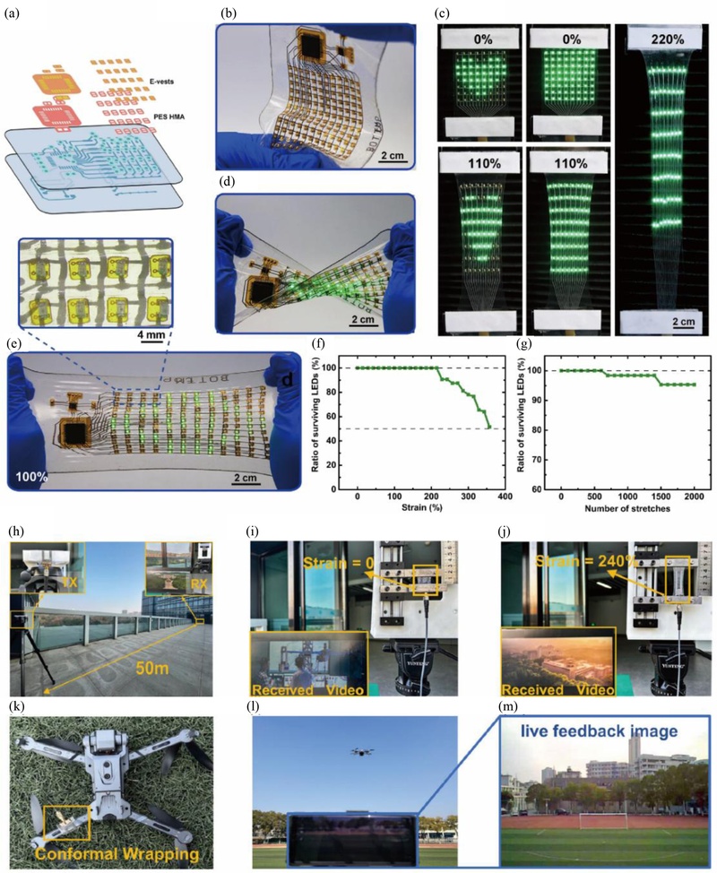
Fig. 9(a) Exploded schematic and assembly process of a stretchable display, (b) Structural details of the soft–rigid interface, (c) Schematic representation of thermal bonding process, (d) Porous PI-based electronic vest structure, (e) Functional mechanism illustration for soft-rigid interconnection, (f) Detailed fabrication procedure of the stretchable display, (g) Survival rate of LEDs under various tensile strains and after cyclic stretching at 100% strain [163], (h) Experimental setup demonstrating wireless video transmission, (i) and (j) Photographs of antenna transmitting video signals before and at 240% mechanical strain, respectively, (k) Photograph of antenna conformally wrapped on drone surface for real-time wireless image transmission, and (l) Real-time wireless transmission demonstration using printed antenna under bending deformation [32] (Adapted from Refs. 32,163 on the basis of OA)
7.3 Stretchable Bioelectronic Systems
Stretchable bioelectronics designed to match biological tissues mechanically and electrically have significant implications for neural stimulation, biosignal monitoring, and self-powered devices [
88,
89]. Recent advancements include AuNW-based stretchable electrodes offering exceptional mechanical compatibility and long-term stability for neural interfaces, significantly improving neurostimulation precision and selectivity [
165]. Advanced stretchable circuits and sensors utilizing hierarchical gold nanowires (AuHNWs) and silver-coated gold nanowires (Ag@AuNWs) have further expanded bioelectronics capabilities, integrating biosignal detection, processing, and output functionalities in flexible, biocompatible configurations.
Stretchable bioelectronics have also advanced beyond traditional skin-mounted devices, extending to complex anatomical structures such as ocular surfaces [
166]. Innovative developments include stretchable corneal sensor systems employing PEDOT-based electrodes directly printed onto soft contact lenses. These sensors enable precise electrophysiological measurements without the need for anesthesia or external instrumentation, markedly enhancing patient comfort and diagnostic accuracy.
These collective advancements in integrated circuits, wireless communications, and bioelectronics form the foundation for next-generation stretchable electronic technologies, providing unprecedented mechanical flexibility, multifunctionality, and integration potential.
8. Challenges and Future Directions in Intrinsically Stretchable Electrode Patterning
Patterning intrinsically stretchable electrodes is fundamental for realizing high-density stretchable electronic devices. Despite significant progress, several critical challenges remain, necessitating strategic research and development to enable practical implementation. This section outlines these challenges and provides focused directions for future advancement.
8.1 High Resolution Combined with Large-area Uniformity
Achieving high-resolution patterning while maintaining uniformity over large-area substrates remains challenging due to factors such as drying kinetics, substrate shrinkage, and uneven surface energy distributions. Developing adaptive methodologies for substrate-process compatibility and large-scale processing strategies will be essential for overcoming these obstacles and enabling consistent high-quality patterning on larger substrates.
8.2 Robust Interfacial Stability in Multilayer Structures
The reliability of multilayer stretchable electronics heavily depends on stable interfaces among heterogeneous functional materials. Challenges such as work-function mismatches, stress concentrations, and varying interfacial wettability can adversely affect device performance. Enhancing interfacial stability will require innovative approaches, including the development of intermediate adhesion layers, low-temperature bonding processes, and stress-relief designs to mitigate these issues.
8.3 Customized Process Optimization for Diverse Materials
Stretchable electrodes incorporate various conductive materials— carbon nanotubes, graphene, metallic nanowires, conductive polymers, MXenes, and liquid metals—each possessing distinct physicochemical properties. Employing a uniform process across different materials can compromise pattern quality and consistency. Tailored ink formulations, precise control of processing parameters, and material-specific solvent systems will be critical for achieving optimal pattern quality and consistent device performance.
8.4 Balancing Stretchability and Precision in Patterning
Despite their ability to withstand substantial mechanical deformation, stretchable materials frequently experience pattern distortion and ink spreading, complicating precise patterning. Maintaining structural integrity and pattern fidelity requires a thorough understanding of multiphysical interactions between material properties, processing conditions, and substrate dynamics, along with precise adjustment of processing parameters to stabilize high-resolution features.
8.5 Sustainable and Low-temperature Processing Techniques
Advancing sustainability and biocompatibility necessitates conductive materials and processing methods that combine high electrical performance with minimal environmental impact. Developing low-temperature, solvent-free, and water-soluble inks, while eliminating high-temperature annealing and volatile organic compounds, represents an important strategic direction toward safer, more sustainable stretchable electronics manufacturing.
8.6 Digital Manufacturing for Integrated Device Platforms
Transitioning from discrete components to fully integrated device systems—including transistors, sensors, interconnects, and circuits—requires advanced digital manufacturing capabilities. Utilizing computer-aided design (CAD)-assisted layouts, conditional printing techniques, and precise multilayer alignment methods will be essential. Leveraging roll-to-roll (R2R) and sheet-to-sheet technologies, alongside high-precision digital processes such as laser sintering and ablation, will enable smart manufacturing and large-scale device production.
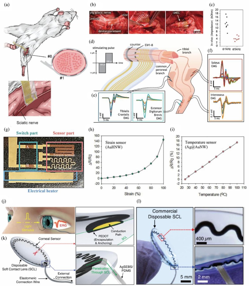
Fig. 10(a) Schematic depicting soft multielectrode cuff placement around a rat sciatic nerve, featuring eight electrodes enabling spatially resolved stimulation [165], (b) Device implantation procedure and positioning illustration, (c) In vivo impedance measurements at 1 kHz and 5 kHz across electrodes #1-#8, (d) Stimulation pulse profiles with current amplitudes from 80 to 800 μA, (e) and (f) Evoked electromyographic (EMG) responses recorded from muscles innervated by the common peroneal (e) and tibial (f) branches of the sciatic nerve [89], (g) Photograph of an integrated multifunctional wearable device, (h) Strain-dependent resistance response of the embedded strain sensor, (i) Temperature-dependent resistance response of the embedded temperature sensor [88], (j) Schematic illustrating human corneal electroretinogram (ERG) recording using a soft contact lens-integrated corneal sensor, (k) Structural schematics highlighting encapsulation and anchoring layers (top inset) and seamless wire connection integration (bottom inset), and (l) Photographs showcasing embedded serpentine electrode design (top inset) and seamless wire integration within the contact lens structure (bottom inset) [166] (Adapted from Ref. 88 with permission and Refs. 89,165,166 on the basis of OA)
Addressing these multifaceted challenges calls for interdisciplinary collaboration among materials science, fluid dynamics, interfacial engineering, and digital manufacturing specialists. Progress in these areas will solidify intrinsically stretchable electrodes as essential elements for future bioelectronics, intelligent robotics, and next-generation wearable healthcare technologies.
9. Conclusion
This review has comprehensively analyzed high-resolution patterning methodologies essential for fabricating intrinsically stretchable electrodes and circuits, pivotal to the advancement of stretchable electronic technologies. While traditional photolithography reliably achieves exceptional resolution, its compatibility with stretchable substrates is limited due to thermal and chemical constraints. In contrast, soft lithography provides significant advantages through cost-effectiveness and low-temperature processing, especially when integrating novel materials such as liquid metals. Laser-based patterning offers notable precision and flexibility in design, though its efficacy strongly depends on optimizing process parameters to match specific material and substrate characteristics. Printing-based techniques provide maskless, non-contact capabilities, accommodating diverse materials and facilitating reliable pattern formation on complex, curved geometries. Furthermore, recent developments in electrospray patterning demonstrate the ability to create high-density, mechanically robust patterns without substrate contact, highlighting its promise for future applications.
The key insights derived from this analysis underscore that no single patterning method universally addresses all requirements for stretchable electronics. Rather, achieving optimal device performance necessitates complementary integration of various patterning processes, tailored specifically to the intrinsic properties and functionalities of different stretchable materials. For instance, hybrid strategies combining photolithography, printing, and laser-based processes have emerged as particularly significant for practical stretchable circuit implementations.
Furthermore, simultaneous realization of mechanical durability and electrical reliability demands in-depth understanding of interactions between materials, processing methods, and substrates. Future development thus requires precise, interaction-aware process designs to achieve both sustained stretchability and conductivity.
Although current research predominantly addresses individual process innovations and small-scale device prototypes, scaling these techniques to large-area, high-throughput, roll-to-roll manufacturing processes represents a critical next step for commercial viability. Advancements in large-area compatibility, coupled with high-speed production techniques, are therefore paramount.
Ultimately, this review establishes a foundational understanding of patterning technologies that will significantly expand the potential applications and performance capabilities of stretchable electronics. These advancements are anticipated to profoundly influence high-impact fields including wearable healthcare, biointerfaces, intelligent robotics, and advanced wireless communication systems. To foster this evolution, integrated interdisciplinary research efforts are necessary, focusing on enhancing resolution, mechanical resilience, and meeting eco-friendly, low-temperature processing, and biocompatibility criteria. The insights and trends highlighted herein aim to serve as vital guidelines for future research directions, driving the practical realization and widespread adoption of stretchable electronic technologies.
ACKNOWLEDGMENTS
The authors would like to acknowledge the financial support from the National Research Foundation of Korea (NRF) (Nos. RS-2023-00222166, RS-2025-00558955).
REFERENCES
- 1.
Lim, C., Hong, Y. J., Jung, J., Shin, Y., Sunwoo, S.-H., Baik, S., Park, O. K., Choi, S. H., Hyeon, T., Kim, J. H., (2021), Tissue-like skin-device interface for wearable bioelectronics by using ultrasoft, mass-permeable, and low-impedance hydrogels, Science Advances, 7(19), eabd3716.
10.1126/sciadv.abd3716
- 2.
Wang, C., Shirzaei Sani, E., Gao, W., (2022), Wearable bioelectronics for chronic wound management, Advanced Functional Materials, 32(17), 2111022.
10.1002/adfm.202111022
- 3.
Gong, S., Lu, Y., Yin, J., Levin, A., Cheng, W., (2024), Materials-driven soft wearable bioelectronics for connected healthcare, Chemical Reviews, 124(2), 455-553.
10.1021/acs.chemrev.3c00502
- 4.
Yang, J. C., Mun, J., Kwon, S. Y., Park, S., Bao, Z., Park, S., (2019), Electronic skin: Recent progress and future prospects for skin‐attachable devices for health monitoring, robotics, and prosthetics, Advanced Materials, 31(48), 1904765.
10.1002/adma.201904765
- 5.
Cho, K. W., Sunwoo, S.-H., Hong, Y. J., Koo, J. H., Kim, J. H., Baik, S., Hyeon, T., Kim, D.-H., (2021), Soft bioelectronics based on nanomaterials, Chemical Reviews, 122(5), 5068-5143.
10.1021/acs.chemrev.1c00531
- 6.
Kim, S. H., Baek, G. W., Yoon, J., Seo, S., Park, J., Hahm, D., Chang, J. H., Seong, D., Seo, H., Oh, S., (2021), A bioinspired stretchable sensory‐neuromorphic system, Advanced Materials, 33(44), 2104690.
10.1002/adma.202104690
- 7.
Zhang, S., Chhetry, A., Zahed, M. A., Sharma, S., Park, C., Yoon, S., Park, J. Y., (2022), On-skin ultrathin and stretchable multifunctional sensor for smart healthcare wearables, npj Flexible Electronics, 6(1), 11.
10.1038/s41528-022-00140-4
- 8.
Park, S., Yuk, H., Zhao, R., Yim, Y. S., Woldeghebriel, E. W., Kang, J., Canales, A., Fink, Y., Choi, G. B., Zhao, X., (2021), Adaptive and multifunctional hydrogel hybrid probes for long-term sensing and modulation of neural activity, Nature Communications, 12(1), 3435.
10.1038/s41467-021-23802-9
- 9.
Zhou, Y., Gu, C., Liang, J., Zhang, B., Yang, H., Zhou, Z., Li, M., Sun, L., Tao, T. H., Wei, X., (2022), A silk-based self-adaptive flexible opto-electro neural probe, Microsystems & Nanoengineering, 8(1), 118.
10.1038/s41378-022-00461-4
- 10.
McDonald, M., Sebinger, D., Brauns, L., Gonzalez-Cano, L., Menuchin-Lasowski, Y., Mierzejewski, M., Psathaki, O.-E., Stumpf, A., Wickham, J., Rauen, T., (2023), A mesh microelectrode array for non-invasive electrophysiology within neural organoids, Biosensors and Bioelectronics, 228, 115223.
10.1016/j.bios.2023.115223
- 11.
Li, T., Li, Y., Zhang, T., (2019), Materials, structures, and functions for flexible and stretchable biomimetic sensors, Accounts of Chemical Research, 52(2), 288-296.
10.1021/acs.accounts.8b00497
- 12.
Xu, K., Lu, Y., Honda, S., Arie, T., Akita, S., Takei, K., (2019), Highly stable kirigami-structured stretchable strain sensors for perdurable wearable electronics, Journal of Materials Chemistry C, 7(31), 9609-9617.
10.1039/C9TC01874C
- 13.
Kim, D. C., Choi, M. K., Kim, D.-H., Yang, J., (2025), Rise of intrinsically stretchable electroluminescent materials: Toward free-form displays, npj Flexible Electronics, 9(1), 50.
10.1038/s41528-025-00427-2
- 14.
Koo, J. H., Yun, H., Lee, W., Sunwoo, S.-H., Shim, H. J., Kim, D.-H. (2022), Recent advances in soft electronic materials for intrinsically stretchable optoelectronic systems, Opto‐Electronic Advances, 5(8), 210131.
10.29026/oea.2022.210131
- 15.
Lee, S., Jeon, Y., Lee, S. Y., Ma, B. S., Song, M., Jeong, D., Jo, J., Kim, G. U., Lee, J., Kim, T. S., (2023), Intrinsically stretchable organic solar cells without cracks under 40% strain, Advanced Energy Materials, 13(30), 2300533.
10.1002/aenm.202300533
- 16.
Barg, I., Kohlmann, N., Rasch, F., Strunskus, T., Adelung, R., Kienle, L., Faupel, F., Schröder, S., Schütt, F., (2023), Strain‐invariant, highly water stable all‐organic soft conductors based on ultralight multi‐layered foam‐like framework structures, Advanced Functional Materials, 33(21), 2212688.
10.1002/adfm.202212688
- 17.
Li, Y., Veronica, A., Ma, J., Nyein, H. Y. Y., (2025), Materials, structure, and interface of stretchable interconnects for wearable bioelectronics, Advanced Materials, 37(23), 2408456.
10.1002/adma.202408456
- 18.
Zhong, D., Wu, C., Jiang, Y., Yuan, Y., Kim, M.-g., Nishio, Y., Shih, C.-C., Wang, W., Lai, J.-C., Ji, X., (2024), High-speed and large-scale intrinsically stretchable integrated circuits, Nature, 627(8003), 313-320.
10.1038/s41586-024-07096-7
- 19.
Zhu, P., Mu, S., Huang, W., Sun, Z., Lin, Y., Chen, K., Pan, Z., Haghighi, M. G., Sedghi, R., Wang, J., (2024), Soft multifunctional neurological electronic skin through intrinsically stretchable synaptic transistor, Nano Research, 17(7), 6550-6559.
10.1007/s12274-024-6566-8
- 20.
Kim, J., Choi, M., Lee, E., (2015), Scalable sub-micron patterning of organic materials toward high density soft electronics, Scientific Reports, 5(1), 14520.
10.1038/srep14520
- 21.
Li, W., Li, L., Sun, Q., Liu, X., Kanehara, M., Nakayama, T., Jiu, J., Sakamoto, K., Minari, T., (2021), Direct fabrication of high-resolution and high-performance flexible electronics via surface-activation-localized electroless plating, Chemical Engineering Journal, 416, 127644.
10.1016/j.cej.2020.127644
- 22.
Jeong, S., Yoon, H., Michalek, L. F., Kim, G., Kim, J., Seo, J., Kim, D., Park, H., Lee, B., Hong, Y., (2024), Printable, stretchable metal-vapor-desorption layers for high-fidelity patterning in soft, freeform electronics, Nature Communications, 15(1), 7209.
10.1038/s41467-024-51585-2
- 23.
Li, F., Fetisova, M., Koskinen, M., Viheriälä, J., Niemi, T., Karvinen, P., Kuittinen, M., (2024), Pattern distortion in nanoimprint lithography using UV-curable polymer stamps, Micro and Nano Engineering, 25, 100293.
10.1016/j.mne.2024.100293
- 24.
Ranka, A., Layek, M., Kochiyama, S., Lopez-Pernia, C., Chandler, A. M., Kocoj, C. A., Magliano, E., Di Carlo, A., Brunetti, F., Guo, P., Suresh, S., Paine D. C., Kesari, H., Padture N. P., (2025), Cracking in polymer substrates for flexible devices and its mitigation, npj Flex Electron 9, 92.
10.1038/s41528-025-00470-z
- 25.
Seiberlich, M., Rainer, C., Skarjan, L., Ruiz‐Preciado, L. A., Perevedentsev, A., Xia, K., Krebsbach, P., Schlisske, S., Lemmer, U., Hernandez‐Sosa, G., (2025), Streamlined inkjet‐printing of stretchable organic photodetectors, Advanced Materials Technologies, 10(10), 2401413.
10.1002/admt.202401413
- 26.
Tian, L., Liu, J., Chen, X., Branicio, P. S., Lei, Q., (2025), Mechanisms and strategies to achieve stability in inkjet printed 2D materials electronics, Advanced Electronic Materials, 11(3), 2400143.
10.1002/aelm.202400143
- 27.
Liang, B., Zhang, Z., Chen, W., Lu, D., Yang, L., Yang, R., Zhu, H., Tang, Z., Gui, X., (2019), Direct patterning of carbon nanotube via stamp contact printing process for stretchable and sensitive sensing devices, Nano-Micro Letters, 11(1), 92.
10.1007/s40820-019-0323-8
- 28.
Xu, F., Zhu, Y., (2012), Highly conductive and stretchable silver nanowire conductors, Advanced Materials, 24(37), 5117-5122.
10.1002/adma.201201886
- 29.
Jeong, S., Heo, S., Kang, M., Kim, H.-J., (2020), Mechanical durability enhancement of gold-nanosheet stretchable electrodes for wearable human bio-signal detection, Materials & Design, 196, 109178.
10.1016/j.matdes.2020.109178
- 30.
Deng, Y., Bu, F., Wang, Y., Chee, P. S., Liu, X., Guan, C., (2024), Stretchable liquid metal based biomedical devices, npj Flexible Electronics, 8(1), 12.
10.1038/s41528-024-00298-z
- 31.
Li, G., Guo, C. F., (2022), PEDOT: PSS-based intrinsically soft and stretchable bioelectronics, Soft Science, 2, 7.
10.20517/ss.2022.07
- 32.
Guo, X., Liu, Y., Zhou, Z., Peng, H., Gao, Y., Shao, M., Yu, Y., (2025), Direct‐ink‐writing printed stretchable eutectic gallium–indium antenna for robust wireless communication, Advanced Science, 2414285.
10.1002/advs.202414285
- 33.
Kim, Y. Y., Yang, T. Y., Suhonen, R., Välimäki, M., Maaninen, T., Kemppainen, A., Jeon, N. J., Seo, J., (2019), Gravure‐printed flexible perovskite solar cells: toward roll‐to‐roll manufacturing, Advanced Science, 6(7), 1802094.
10.1002/advs.201802094
- 34.
Al-Milaji, K. N., Huang, Q., Li, Z., Ng, T. N., Zhao, H., (2020), Direct embedment and alignment of silver nanowires by inkjet printing for stretchable conductors, ACS Applied Electronic Materials, 2(10), 3289-3298.
10.1021/acsaelm.0c00616
- 35.
Zhao, C., Zhou, Y., Gu, S., Cao, S., Wang, J., Zhang, M., Wu, Y., Kong, D., (2020), Fully screen-printed, multicolor, and stretchable electroluminescent displays for epidermal electronics, ACS Applied Materials & Interfaces, 12(42), 47902-47910.
10.1021/acsami.0c12415
- 36.
Lienemann, S., Zötterman, J., Farnebo, S., Tybrandt, K., (2021), Stretchable gold nanowire-based cuff electrodes for low-voltage peripheral nerve stimulation, Journal of Neural Engineering, 18(4), 045007.
10.1088/1741-2552/abfebb
- 37.
Kweon, H., Choi, K.-Y., Park, H. W., Lee, R., Jeong, U., Kim, M. J., Hong, H., Ha, B., Lee, S., Kwon, J.-Y., (2022), Silicone engineered anisotropic lithography for ultrahigh-density OLEDs, Nature Communications, 13(1), 6775.
10.1038/s41467-022-34531-y
- 38.
Lunghi, A., Mariano, A., Bianchi, M., Dinger, N. B., Murgia, M., Rondanina, E., Toma, A., Greco, P., Di Lauro, M., Santoro, F., (2022), Flexible neural interfaces based on 3D PEDOT: PSS micropillar arrays, Advanced Materials Interfaces, 9(25), 2200709.
10.1002/admi.202200709
- 39.
Park, S. H., Lei, L., D’Souza, D., Zipkin, R., DiMartini, E. T., Atzampou, M., Lallow, E. O., Shan, J. W., Zahn, J. D., Shreiber, D. I., (2023), Efficient electrospray deposition of surfaces smaller than the spray plume, Nature Communications, 14(1), 4896.
10.1038/s41467-023-40638-7
- 40.
Kim, K.-W., Park, S. J., Park, S.-J., Kim, I., Park, B., Kim, S. H., Jeong, U., Kim, J. K., Yang, C., (2024), Deformable micro-supercapacitor fabricated via laser ablation patterning of Graphene/liquid metal, npj Flexible Electronics, 8(1), 18.
10.1038/s41528-024-00306-2
- 41.
Eiroma, K., Sneck, A., Halonen, O., Happonen, T., Sandberg, H., Leppaniemi, J., (2025), Miniaturized micrometer-level copper wiring and electrodes based on reverse-offset printing for flexible circuits, ACS Applied Electronic Materials, 7(8), 3511-3520.
10.1021/acsaelm.5c00230
- 42.
Hu, X., Feng, J., Zhang, H., Ma, J., Wu, Z., Wen, J., Wang, S., Tian, Y., (2023), Electrohydrodynamic printing of high‐resolution self‐reduced soldered silver nanowire pattern for wearable flexible strain sensors, Advanced Materials Technologies, 8(19), 2300759.
10.1002/admt.202300759
- 43.
Lapinski, N., Liu, Z., Yang, S., Hui, C.-Y., Jagota, A., (2019), A surface with stress, extensional elasticity, and bending stiffness, Soft Matter, 15(18), 3817-3827.
10.1039/C9SM00075E
- 44.
Yoo, D., Won, D. J., Cho, W., Kim, S., Kim, J., (2021), High‐resolution and facile patterning of silver nanowire electrodes by solvent‐free photolithographic technique using uv‐curable pressure sensitive adhesive film, Small Methods, 5(12), 2101049.
10.1002/smtd.202101049
- 45.
Zhou, H., Mao, H., Meng, X., Wang, Q., Tan, L., Chen, Y., (2019), Electroless deposition of silver grids flexible transparent electrode integrated by ultra-violet nanoimprint lithography, Organic Electronics, 75, 105408.
10.1016/j.orgel.2019.105408
- 46.
An, E. Y., Lee, S., Lee, S. G., Lee, E., Baek, J. J., Shin, G., Choi, K. H., Cho, J. H., Bae, G. Y., (2021), Self-patterned stretchable electrode based on silver nanowire bundle mesh developed by liquid bridge evaporation, Nanomaterials, 11(11), 2865.
10.3390/nano11112865
- 47.
Park, Y., Jung, J., Lee, Y., Lee, D., Vlassak, J. J., Park, Y.-L., (2022), Liquid-metal micro-networks with strain-induced conductivity for soft electronics and robotic skin, npj Flexible Electronics, 6(1), 81.
10.1038/s41528-022-00215-2
- 48.
Liu, S., Kim, S. Y., Henry, K. E., Shah, D. S., Kramer-Bottiglio, R., (2021), Printed and laser-activated liquid metal-elastomer conductors enabled by ethanol/PDMS/liquid metal double emulsions, ACS Applied Materials & Interfaces, 13(24), 28729-28736.
10.1021/acsami.0c23108
- 49.
Won, D., Kim, J., Choi, J., Kim, H., Han, S., Ha, I., Bang, J., Kim, K. K., Lee, Y., Kim, T.-S., (2022), Digital selective transformation and patterning of highly conductive hydrogel bioelectronics by laser-induced phase separation, Science Advances, 8(23), eabo3209.
10.1126/sciadv.abo3209
- 50.
Xiao, P., Kim, J.-H., Seo, S., (2021), Flexible and stretchable liquid metal electrodes working at sub-zero temperature and their applications, Materials, 14(15), 4313.
10.3390/ma14154313
- 51.
Zhao, Y., Zhang, L., Lv, M., Jiao, C., Cheng, P., Fu, Y., Li, J., Liu, Q., He, D., (2021), Improvement of the optoelectrical properties of a transparent conductive polymer via the introduction of ito nanoparticles and its application in crystalline silicon/organic heterojunction solar cells, ACS Applied Materials & Interfaces, 13(26), 31171-31179.
10.1021/acsami.1c07415
- 52.
Kim, M.-g., Brown, D. K., Brand, O., (2020), Nanofabrication for all-soft and high-density electronic devices based on liquid metal, Nature Communications, 11(1), 1002.
10.1038/s41467-020-14814-y
- 53.
Sun, Y.-C., Boero, G., Brugger, J. R., (2021), Stretchable conductors fabricated by stencil lithography and centrifugal force-assisted patterning of liquid metal, ACS Applied Electronic Materials, 3(12), 5423-5432.
10.1021/acsaelm.1c00884
- 54.
Basak, I., Nowicki, G., Ruttens, B., Desta, D., Prooth, J., Jose, M., Nagels, S., Boyen, H.-G., D’Haen, J., Buntinx, M., (2020), Inkjet printing of PEDOT: PSS based conductive patterns for 3D forming applications, Polymers, 12(12), 2915.
10.3390/polym12122915
- 55.
Van Hazendonk, L. S., Pinto, A. M., Arapov, K., Pillai, N., Beurskens, M. R., Teunissen, J.-P., Sneck, A., Smolander, M., Rentrop, C. H., Bouten, P. C., (2022), Printed stretchable graphene conductors for wearable technology, Chemistry of Materials, 34(17), 8031-8042.
10.1021/acs.chemmater.2c02007
- 56.
Hassan, R. U., Khalil, S. M., Khan, S. A., Ali, S., Moon, J., Cho, D.-H., Byun, D., (2022), High-resolution, transparent, and flexible printing of polydimethylsiloxane via electrohydrodynamic jet printing for conductive electronic device applications, Polymers, 14(20), 4373.
10.3390/polym14204373
- 57.
Lin, Y., Li, Q., Ding, C., Wang, J., Yuan, W., Liu, Z., Su, W., Cui, Z., (2022), High-resolution and large-size stretchable electrodes based on patterned silver nanowires composites, Nano Research, 15(5), 4590-4598.
10.1007/s12274-022-4088-x
- 58.
Boda, U., Strandberg, J., Eriksson, J., Liu, X., Beni, V., Tybrandt, K., (2023), Screen-printed corrosion-resistant and long-term stable stretchable electronics based on agau microflake conductors, ACS Applied Materials & Interfaces, 15(9), 12372-12382.
10.1021/acsami.2c22199
- 59.
Park, J. E., Kang, H. S., Koo, M., Park, C., (2020), Autonomous surface reconciliation of a liquid‐metal conductor micropatterned on a deformable hydrogel, Advanced Materials, 32(37), 2002178.
10.1002/adma.202002178
- 60.
Giannopoulos, I., Mochi, I., Vockenhuber, M., Ekinci, Y., Kazazis, D., (2024), Extreme ultraviolet lithography reaches 5 nm resolution, Nanoscale, 16(33), 15533-15543.
10.1039/D4NR01332H
- 61.
Lim, K., Seo, H., Chung, W. G., Song, H., Oh, M., Ryu, S. Y., Kim, Y., Park, J.-U., (2024), Material and structural considerations for high-performance electrodes for wearable skin devices, Communications Materials, 5(1), 49.
10.1038/s43246-024-00490-8
- 62.
Hou, S., Chen, C., Bai, L., Yu, J., Cheng, Y., Huang, W., (2024), Stretchable electronics with strain‐resistive performance, Small, 20(11), 2306749.
10.1002/smll.202306749
- 63.
Kang, G. R., Hwang, G. W., Lim, D., Jeon, S. H., Song, M., Hong, C. H., Kim, H. J., Pang, C., (2025), Robustly repeatable, permeable, and multi‐axially stretchable, adhesive bioelectronics with super‐adaptive conductive suction cups for continuously deformable biosurfaces, Advanced Science, 12(25), 2500346.
10.1002/advs.202500346
- 64.
Zhou, Y., Azumi, R., Shimada, S., (2019), A highly durable, stretchable, transparent and conductive carbon nanotube–polymeric acid hybrid film, Nanoscale, 11(9), 3804-3813.
10.1039/C8NR08399A
- 65.
Yan, Z., Wang, L., Xia, Y., Qiu, R., Liu, W., Wu, M., Zhu, Y., Zhu, S., Jia, C., Zhu, M., (2021), Flexible high‐resolution triboelectric sensor array based on patterned laser‐induced graphene for self‐powered real‐time tactile sensing, Advanced Functional Materials, 31(23), 2100709.
10.1002/adfm.202100709
- 66.
Qiao, Y., Li, X., Wang, J., Ji, S., Hirtz, T., Tian, H., Jian, J., Cui, T., Dong, Y., Xu, X., (2022), Intelligent and multifunctional graphene nanomesh electronic skin with high comfort, Small, 18(7), 2104810.
10.1002/smll.202104810
- 67.
Kumar, V., Alam, M. N., Park, S. S., (2024), Review on functionalized cnts reinforced silicone rubber composites for potential wearable applications, Polymer Composites, 45(14), 12503-12529.
10.1002/pc.28664
- 68.
Guo, C. F., Sun, T., Liu, Q., Suo, Z., Ren, Z., (2014), Highly stretchable and transparent nanomesh electrodes made by grain boundary lithography, Nature Communications, 5(1), 3121.
10.1038/ncomms4121
- 69.
Wang, Y., Gong, S., Wang, S. J., Yang, X., Ling, Y., Yap, L. W., Dong, D., Simon, G. P., Cheng, W., (2018), Standing enokitake-like nanowire films for highly stretchable elastronics, ACS Nano, 12(10), 9742-9749.
10.1021/acsnano.8b05019
- 70.
Yu, K., He, T., (2023), Silver-nanowire-based elastic conductors: Preparation processes and substrate adhesion, Polymers, 15(6), 1545.
10.3390/polym15061545
- 71.
Zhu, H., Wang, S., Zhang, M., Li, T., Hu, G., Kong, D., (2021), Fully solution processed liquid metal features as highly conductive and ultrastretchable conductors, npj Flexible Electronics, 5(1), 25.
10.1038/s41528-021-00123-x
- 72.
Choi, H., Luo, Y., Olson, G., Won, P., Shin, J. H., Ok, J., Yang, Y. J., Kim, T. I., Majidi, C., (2023), Highly stretchable and strain‐insensitive liquid metal based elastic kirigami electrodes (LM‐eKE), Advanced Functional Materials, 33(30), 2301388.
10.1002/adfm.202301388
- 73.
Vallem, V., Aggarwal, V., Dickey, M. D., (2023), Stretchable liquid metal films with high surface area and strain invariant resistance, Advanced Materials Technologies, 8(5), 2201233.
10.1002/admt.202201233
- 74.
Wang, Y., Zhu, C., Pfattner, R., Yan, H., Jin, L., Chen, S., Molina-Lopez, F., Lissel, F., Liu, J., Rabiah, N. I., (2017), A highly stretchable, transparent, and conductive polymer, Science Advances, 3(3), e1602076.
10.1126/sciadv.1602076
- 75.
Li, G., Qiu, Z., Wang, Y., Hong, Y., Wan, Y., Zhang, J., Yang, J., Wu, Z., Hong, W., Guo, C. F., (2019), PEDOT: PSS/grafted-pdms electrodes for fully organic and intrinsically stretchable skin-like electronics, ACS Applied Materials & Interfaces, 11(10), 10373-10379.
10.1021/acsami.8b20255
- 76.
Kim, Y., Yoo, S., Kim, J.-H., (2022), Water-based highly stretchable PEDOT: PSS/nonionic WPU transparent electrode, Polymers, 14(5), 949.
10.3390/polym14050949
- 77.
Kelly, A. G., Sheil, S., Douglas-Henry, D. A., Caffrey, E., Gabbett, C., Doolan, L., Nicolosi, V., Coleman, J. N., (2023), Transparent conductors printed from grids of highly conductive silver nanosheets, ACS Applied Materials & Interfaces, 15(33), 39864-39871.
10.1021/acsami.3c07459
- 78.
Kwon, N. Y., Park, S. H., Lee, Y., Kong, G. D., Chau, H. D., Yoon, H. J., Woo, H. Y., Hoang, M. H., Cho, M. J., Choi, D. H., (2022), Uniform silver nanowire patterned electrode on robust PEN substrate using poly (2-hydroxyethyl methacrylate) underlayer, ACS Applied Materials & Interfaces, 14(30), 34909-34917.
10.1021/acsami.2c07063
- 79.
Nguyen, T., Khine, M., (2020), Advances in Materials for Soft Stretchable Conductors and Their Behavior under Mechanical Deformation, Polymers, 12(7), 1454.
10.3390/polym12071454
- 80.
Bian, Y., Zhu, M., Wang, C., Liu, K., Shi, W., Zhu, Z., Qin, M., Zhang, F., Zhao, Z., Wang, H., (2024), A detachable interface for stable low-voltage stretchable transistor arrays and high-resolution X-ray imaging, Nature Communications, 15(1), 2624.
10.1038/s41467-024-47026-9
- 81.
Min, S.-H., Lee, G.-Y., Ahn, S.-H., (2019), Direct printing of highly sensitive, stretchable, and durable strain sensor based on silver nanoparticles/multi-walled carbon nanotubes composites, Composites Part B: Engineering, 161, 395-401.
10.1016/j.compositesb.2018.12.107
- 82.
Go, M., Qi, X., Matteini, P., Hwang, B., Lim, S., (2021), High resolution screen-printing of carbon black/carbon nanotube composite for stretchable and wearable strain sensor with controllable sensitivity, Sensors and Actuators A: Physical, 332, 113098.
10.1016/j.sna.2021.113098
- 83.
Shi, G., Lowe, S. E., Teo, A. J., Dinh, T. K., Tan, S. H., Qin, J., Zhang, Y., Zhong, Y. L., Zhao, H., (2019), A versatile pdms submicrobead/graphene oxide nanocomposite ink for the direct ink writing of wearable micron-scale tactile sensors, Applied Materials Today, 16, 482-492.
10.1016/j.apmt.2019.06.016
- 84.
Kong, X., Li, H., Wang, J., Wang, Y., Zhang, L., Gong, M., Lin, X., Wang, D., (2023), Direct writing of silver nanowire patterns with line width down to 50 μm and ultrahigh conductivity, ACS Applied Materials & Interfaces, 15(7), 9906-9915.
10.1021/acsami.2c22885
- 85.
Matsuhisa, N., Niu, S., O’Neill, S. J., Kang, J., Ochiai, Y., Katsumata, T., Wu, H.-C., Ashizawa, M., Wang, G.-J. N., Zhong, D., (2021), High-frequency and intrinsically stretchable polymer diodes, Nature, 600(7888), 246-252.
10.1038/s41586-021-04053-6
- 86.
Song, J. Y., Oh, J. H., Choi, D., Park, S. M., (2021), Highly efficient patterning technique for silver nanowire electrodes by electrospray deposition and its application to self-powered triboelectric tactile sensor, Scientific Reports, 11(1), 21437.
10.1038/s41598-021-01043-6
- 87.
Tian, B., Fang, Y., Liang, J., Zheng, K., Guo, P., Zhang, X., Wu, Y., Liu, Q., Huang, Z., Cao, C., (2022), Fully printed stretchable and multifunctional e‐textiles for aesthetic wearable electronic systems, Small, 18(13), 2107298.
10.1002/smll.202107298
- 88.
Kim, T. Y., Hong, S. H., Jeong, S. H., Bae, H., Cheong, S., Choi, H., Hahn, S. K., (2023), Multifunctional intelligent wearable devices using logical circuits of monolithic gold nanowires, Advanced Materials, 35(45), 2303401.
10.1002/adma.202303401
- 89.
Lienemann, S., Donahue, M. J., Zötterman, J., Farnebo, S., Tybrandt, K., (2023), A soft and stretchable multielectrode cuff for selective peripheral nerve stimulation, Advanced Materials Technologies, 8(6), 2201322.
10.1002/admt.202201322
- 90.
Kim, M., Cho, C., Shin, W., Park, J. J., Kim, J., Won, P., Majidi, C., Ko, S. H., (2022), Nanowire-assisted freestanding liquid metal thin-film patterns for highly stretchable electrodes on 3D surfaces, npj Flexible Electronics, 6(1), 99.
10.1038/s41528-022-00232-1
- 91.
Zhang, J.-R., Li, A., Li, X.-L., Zhao, Y.-B., Sun, J.-S., Guo, X.-X., Wang, W., Liu, J., Zhang, Y.-L., Han, D.-D., (2025), High-resolution stretchable soft liquid metal circuits based on Cu-Ga alloying and femtosecond laser ablation, ACS Applied Materials & Interfaces, 17(12), 18940-18953.
10.1021/acsami.5c01934
- 92.
Liu, S., Shah, D. S., Kramer-Bottiglio, R., (2021), Highly stretchable multilayer electronic circuits using biphasic gallium-indium, Nature Materials, 20(6), 851-858.
10.1038/s41563-021-00921-8
- 93.
Park, Y.-G., Min, H., Kim, H., Zhexembekova, A., Lee, C. Y., Park, J.-U., (2019), Three-dimensional, high-resolution printing of carbon nanotube/liquid metal composites with mechanical and electrical reinforcement, Nano Letters, 19(8), 4866-4872.
10.1021/acs.nanolett.9b00150
- 94.
Wu, D., Wu, S., Narongdej, P., Duan, S., Chen, C., Yan, Y., Liu, Z., Hong, W., Frenkel, I., He, X., (2024), Fast and facile liquid metal printing via projection lithography for highly stretchable electronic circuits, Advanced Materials, 36(34), 2307632.
10.1002/adma.202307632
- 95.
Zhuang, Q., Yao, K., Wu, M., Lei, Z., Chen, F., Li, J., Mei, Q., Zhou, Y., Huang, Q., Zhao, X., (2023), Wafer-patterned, permeable, and stretchable liquid metal microelectrodes for implantable bioelectronics with chronic biocompatibility, Science Advances, 9(22), eadg8602.
10.1126/sciadv.adg8602
- 96.
Lopes, P. A., Fernandes, D. F., Silva, A. F., Marques, D. G., de Almeida, A. T., Majidi, C., Tavakoli, M., (2021), Bi-phasic Ag–In–Ga-embedded elastomer inks for digitally printed, ultra-stretchable, multi-layer electronics, ACS Applied Materials & Interfaces, 13(12), 14552-14561.
10.1021/acsami.0c22206
- 97.
Hou, S., Chen, H., Lv, D., Li, W., Liu, X., Zhang, Q., Yu, X., Han, Y., (2023), Highly conductive inkjet-printed PEDOT: PSS film under cyclic stretching, ACS Applied Materials & Interfaces, 15(23), 28503-28515.
10.1021/acsami.3c03378
- 98.
Yoon, S. J., Ha, J., Lee, H., Park, J. T., Lee, B. H., Jang, K.-I., Yang, A., Lee, Y. K., (2024), Water-based direct photopatterning of stretchable PEDOT: PSS using amphiphilic block copolymers, npj Flexible Electronics, 8(1), 22.
10.1038/s41528-024-00308-0
- 99.
Yu, X., Mahajan, B. K., Shou, W., Pan, H., (2016), Materials, mechanics, and patterning techniques for elastomer-based stretchable conductors, Micromachines, 8(1), 7.
10.3390/mi8010007
- 100.
Stier, S. P., Böse, H., (2021), Electroplating and ablative laser structuring of elastomer composites for stretchable multi-layer and multi-material electronic and sensor systems, Micromachines, 12(3), 255.
10.3390/mi12030255
- 101.
Sumaria, K., Liu, T. L., (2025), A Subtractive Method to Chemically Pattern Liquid Metal for Stretchable Circuits, Advanced Materials Technologies, 10(3), 2401200.
10.1002/admt.202401200
- 102.
Choi, A., Hoang, A. T., Van, T. T. N., Shong, B., Hu, L., Thai, K. Y., Ahn, J.-H., (2022), Residue-free photolithographic patterning of graphene, Chemical Engineering Journal, 429, 132504.
10.1016/j.cej.2021.132504
- 103.
Bathaei, M. J., Singh, R., Mirzajani, H., Istif, E., Akhtar, M. J., Abbasiasl, T., Beker, L., (2023), Photolithography‐based microfabrication of biodegradable flexible and stretchable sensors, Advanced Materials, 35(6), 2207081.
10.1002/adma.202207081
- 104.
Liu, X., Dai, S., Zhao, W., Zhang, J., Guo, Z., Wu, Y., Xu, Y., Sun, T., Li, L., Guo, P., (2024), All‐photolithography fabrication of ion‐gated flexible organic transistor array for multimode neuromorphic computing, Advanced Materials, 36(21), 2312473.
10.1002/adma.202312473
- 105.
Zhong, D., Nishio, Y., Wu, C., Jiang, Y., Wang, W., Yuan, Y., Yao, Y., Tok, J. B.-H., Bao, Z., (2024), Design considerations and fabrication protocols of high-performance intrinsically stretchable transistors and integrated circuits, ACS Nano, 18(48), 33011-33031.
10.1021/acsnano.4c14026
- 106.
Guo, Q., Xu, Z., Yang, L., Zhang, J., Gan, Y., Zhang, J., Jiang, J., Wang, Y., (2025), High-precision and wafer-scale transfer lithography of commercial photoresists via reversible adhesion for sustainable microfabrication on diverse substrates, arXiv:
2504.15078.
- 107.
Chen, J., Yi, D., Ren, Y., Zhou, X., Qi, Z. Y., Zhang, X. Y., Shang, L., Yao, J., Shen, B., Zheng, W., (2025), Porous elastomer film with controlled liquid‐metal distribution for recyclable highly customizable and stretchable patterned electronics, Advanced Materials, 37(37), 2505839.
10.1002/adma.202505839
- 108.
Song, T. E., Yun, H., Kim, Y. J., Jeon, H. S., Ha, K., Jung, H. T., Han, H., Gogotsi, Y., Ahn, C. W., Lee, Y., (2020), Vertically aligned nanopatterns of amine‐functionalized Ti3C2 MXene via soft lithography, Advanced Materials Interfaces, 7(18), 2000424.
10.1002/admi.202000424
- 109.
Liu, Y., Zheng, M., O’Connor, B., Dong, J., Zhu, Y., (2022), Curvilinear soft electronics by micromolding of metal nanowires in capillaries, Science Advances, 8(46), eadd6996.
10.1126/sciadv.add6996
- 110.
Namkoong, M., Guo, H., Rahman, M. S., Wang, D., Pfeil, C. J., Hager, S., Tian, L., (2022), Moldable and transferrable conductive nanocomposites for epidermal electronics, npj Flexible Electronics, 6(1), 41.
10.1038/s41528-022-00170-y
- 111.
Rosenberg, M., Schvartzman, M., (2019), Direct resistless soft nanopatterning of freeform surfaces, ACS Applied Materials & Interfaces, 11(46), 43494-ss43499.
10.1021/acsami.9b13494
- 112.
Szuwarzyński, M., Mazur, Ł., Borkowski, M., Maćkosz, K., Giżyński, K., Mazur, T., (2022), Enhanced assembly of Ag nanoparticles for surface-independent fabrication of conductive patterns, ACS Applied Nano Materials, 5(9), 12711-12719.
10.1021/acsanm.2c02559
- 113.
Zhang, J., Zhang, C., Li, H., Cheng, Y., Yang, Q., Hou, X., Chen, F., (2022), Controlling the oxidation and wettability of liquid metal via femtosecond laser for high-resolution flexible electronics, Frontiers in Chemistry, 10, 965891.
10.3389/fchem.2022.965891
- 114.
Babatain, W., Park, C., Ishii, H., Gershenfeld, N., (2025), Laser‐enabled fabrication of flexible printed electronics with integrated functional devices, Advanced Science, 12(20), 2415272.
10.1002/advs.202415272
- 115.
Guo, X., Hong, W., Zhao, Y., Zhu, T., Liu, L., Li, H., Wang, Z., Wang, D., Mai, Z., Zhang, T., (2023), Bioinspired dual‐mode stretchable strain sensor based on magnetic nanocomposites for strain/magnetic discrimination, Small, 19(1), 2205316.
10.1002/smll.202205316
- 116.
Lin, Y., Yuan, W., Ding, C., Chen, S., Su, W., Hu, H., Cui, Z., Li, F., (2020), Facile and efficient patterning method for silver nanowires and its application to stretchable electroluminescent displays, ACS Applied Materials & Interfaces, 12(21), 24074-24085.
10.1021/acsami.9b21755
- 117.
Wang, C., Linghu, C., Nie, S., Li, C., Lei, Q., Tao, X., Zeng, Y., Du, Y., Zhang, S., Yu, K., (2020), Programmable and scalable transfer printing with high reliability and efficiency for flexible inorganic electronics, Science Advances, 6(25), eabb2393.
10.1126/sciadv.abb2393
- 118.
Cui, S., Sun, K., Liao, Z., Zhou, Q., Jin, L., Jin, C., Hu, J., Wen, K.-S., Liu, S., Zhou, S., (2024), Flexible nanoimprint lithography enables high-throughput manufacturing of bioinspired microstructures on warped substrates for efficient III-nitride optoelectronic devices, Science Bulletin, 69(13), 2080-2088.
10.1016/j.scib.2024.04.030
- 119.
Savari, H., Nikfarjam, A., (2024), Design and fabrication of patterned flexible electrode using DC sputtering and shadow mask, Engineering Research Express, 6(4), 045318.
10.1088/2631-8695/ad833a
- 120.
Li, D., Cui, J., An, C., Liu, Q., Xu, J., Han, X., Yang, S., Lai, W. Y., (2025), Screen‐printed PEDOT: PSS/Ag composite electrodes for high‐performance paper‐based supercapacitors, Advanced Sustainable Systems, e00131.
10.1002/adsu.202500131
- 121.
Zhou, W., Yao, S., Wang, H., Du, Q., Ma, Y., Zhu, Y., (2020), Gas-permeable, ultrathin, stretchable epidermal electronics with porous electrodes, ACS Nano, 14(5), 5798-5805.
10.1021/acsnano.0c00906
- 122.
Zhu, M., Mao, Y., (2025), Substrate-independent wettability patterning via vapor-based polymer nanocoating deposition for enhanced droplet transport, ACS Applied Polymer Materials, 7(4), 2451-2458.
10.1021/acsapm.4c03577
- 123.
Kim, J.-H., Kim, S., Kim, H., Wooh, S., Cho, J., Dickey, M. D., So, J.-H., Koo, H.-J., (2022), Imbibition-induced selective wetting of liquid metal, Nature Communications, 13(1), 4763.
10.1038/s41467-022-32259-3
- 124.
Prakash, C. J., Lee, J.-W., (2023), Selective de-silanization assisted wettability patterning of aluminum surfaces, Journal of Materials Science, 58(15), 6775-6783.
10.1007/s10853-023-08432-4
- 125.
Ma, P., Wang, Y., Wang, J., Xue, L., Lin, Y., Dong, Y., Chen, P., Du, W., Li, Y., Liu, B.-F., (2023), Wax-shaped wettability assisted patterning of silver nanowires on various substrates as transparent, flexible, or stretchable electrodes, Applied Surface Science, 639, 158232.
10.1016/j.apsusc.2023.158232
- 126.
Yang, J. C., Kim, J.-O., Oh, J., Kwon, S. Y., Sim, J. Y., Kim, D. W., Choi, H. B., Park, S., (2019), Microstructured porous pyramid-based ultrahigh sensitive pressure sensor insensitive to strain and temperature, ACS Applied Materials & Interfaces, 11(21), 19472-19480.
10.1021/acsami.9b03261
- 127.
Vu, H. H., Nguyen, N.-T., Nguyen, N.-K., Luu, C. H., Hettiarachchi, S., Kashaninejad, N., (2023), Tunable wettability with stretchable microstructured surfaces, Advanced Engineering Materials, 25(23), 2300821.
10.1002/adem.202300821
- 128.
Clark, K. M., Nekoba, D. T., Viernes, K. L., Zhou, J., Ray, T. R., (2024), Fabrication of high-resolution, flexible, laser-induced graphene sensors via stencil masking, Biosensors and Bioelectronics, 264, 116649.
10.1016/j.bios.2024.116649
- 129.
Wang, M., Ma, C., Uzabakiriho, P. C., Chen, X., Chen, Z., Cheng, Y., Wang, Z., Zhao, G., (2021), Stencil printing of liquid metal upon electrospun nanofibers enables high-performance flexible electronics, ACS Nano, 15(12), 19364-19376.
10.1021/acsnano.1c05762
- 130.
Wang, H., Guo, R., Li, H., Wang, J., Du, C., Wang, X., Zheng, Z., (2022), 2D metal patterns transformed from 3D printed stamps for flexible Zn//MnO2 in-plane micro-batteries, Chemical Engineering Journal, 429, 132196.
10.1016/j.cej.2021.132196
- 131.
Volkert, C., Colucci, R., Berger, R., Besenius, P., Blom, P. W., Kraft, U., (2024), Transfer-printing of patterned PEDOT: PSS structures for bendable, stretchable and biodegradable electronics, Journal of Materials Chemistry C, 12(11), 3865-3872.
10.1039/D3TC04485H
- 132.
Yang, J., Chang, L., Zhao, H., Zhang, X., Cao, Z., Jiang, L., (2024), Multilayer ordered silver nanowire network films by self‐driven climbing for large‐area flexible optoelectronic devices, InfoMat, 6(5), e12529.
10.1002/inf2.12529
- 133.
Liu, L., Shen, Z., Zhang, X., Ma, H., (2021), Highly conductive graphene/carbon black screen printing inks for flexible electronics, Journal of Colloid and Interface Science, 582, Part A, 12-21.
10.1016/j.jcis.2020.07.106
- 134.
Tang, X., Wu, K., Qi, X., Kwon, H.-j., Wang, R., Li, Z., Ye, H., Hong, J., Choi, H. H., Kong, H., (2022), Screen printing of silver and carbon nanotube composite inks for flexible and reliable organic integrated devices, ACS Applied Nano Materials, 5(4), 4801-4811.
10.1021/acsanm.1c04317
- 135.
Shukla, D., Liu, Y., Zhu, Y., (2023), Eco-friendly screen printing of silver nanowires for flexible and stretchable electronics, Nanoscale, 15(6), 2767-2778.
10.1039/D2NR05840E
- 136.
Shang, J., Mohammadi, M., Strandberg, J., Petsagkourakis, I., Åhlin, J., Hagel, O., Yi, Y., Herlogsson, L., Tybrandt, K., (2025), Fully screen printed stretchable liquid metal multilayer circuits using green solvents and scalable water-spray sintering, npj Flexible Electronics, 9(1), 19.
10.1038/s41528-025-00394-8
- 137.
Wang, S., Wang, Q., Li, M., Fang, Y., Shao, S., Xie, T., Zhao, C., Liang, L., Zhao, J., (2023), Roll-to-roll gravure printed large-area flexible carbon nanotube synaptic photogating transistor arrays for image recognitions, Nano Energy, 115, 108698.
10.1016/j.nanoen.2023.108698
- 138.
Ma, S., Dahiya, A. S., Christou, A., Zumeit, A., Dahiya, R., (2024), High‐resolution printing‐based vertical interconnects for flexible hybrid electronics, Advanced Materials Technologies, 9(17), 2400130.
10.1002/admt.202400130
- 139.
Wang, H., Pan, Y., Han, Y., Chen, Z., Liu, T., Zhang, L., Luo, Q., Ma, C. Q., (2024), Large‐area gravure‐printed AgNWs electrode on water/oxygen barrier substrate for long‐term stable large‐area flexible organic solar cells, Chinese Journal of Chemistry, 42(5), 478-484.
10.1002/cjoc.202300479
- 140.
Kawakami, H., Nagatake, K., Ni, S., Nakamura, F., Takano, T., Murakami, K., Ohara, I., Isano, Y., Matsuda, R., Suwa, H., (2024), R2R‐based continuous production of patterned and multilayered elastic substrates with liquid metal wiring for stretchable electronics, Advanced Materials Technologies, 9(17), 2400487.
10.1002/admt.202400487
- 141.
Kang, D., Kim, H., Kim, H., Jo, J., Lee, T.-M., (2022), Actively compensated precision overlay in a reverse-offset printing system for realizing printed electronics of a large-area and multi-layer structure, Flexible and Printed Electronics, 7(1), 014010.
10.1088/2058-8585/ac5213
- 142.
Dai, H., Xia, Y., Beeby, S., Torah, R., (2025), High‐resolution reverse offset printed electroluminescent multipixel arrays for scalable future wearable displays, Advanced Engineering Materials, 27(17), 2500582.
10.1002/adem.202500582
- 143.
Kim, J., Hwang, I., Kim, M., Jung, H., Bae, H., Lee, Y., (2022), Simple, fast, and scalable reverse-offset printing of micropatterned copper nanowire electrodes with sub-10 μm resolution, ACS Applied Materials & Interfaces, 14(4), 5807-5814.
10.1021/acsami.1c21223
- 144.
Lo, L.-W., Zhao, J., Wan, H., Wang, Y., Chakrabartty, S., Wang, C., (2021), An inkjet-printed PEDOT: PSS-based stretchable conductor for wearable health monitoring device applications, ACS Applied Materials & Interfaces, 13(18), 21693-21702.
10.1021/acsami.1c00537
- 145.
Silva, A. F., Paisana, H., Fernandes, T., Góis, J., Serra, A., Coelho, J. F., de Almeida, A. T., Majidi, C., Tavakoli, M., (2020), High resolution soft and stretchable circuits with PVA/liquid‐metal mediated printing, Advanced Materials Technologies, 5(9), 2000343.
10.1002/admt.202000343
- 146.
Jeong, S., Yoon, H., Michalek, L. F., Kim, G., Kim, J., Seo, J., Kim, D., Park, H., Lee, B., Hong, Y., (2024), Printable, stretchable metal-vapor-desorption layers for high-fidelity patterning in soft, freeform electronics, Nature Communications, 15(1), 7209.
10.1038/s41467-024-51585-2
- 147.
Cho, Y., Kim, K., Kim, D., Bissannagari, M., Lee, J., Hong, W., Kwon, H.-J., Jang, J. E., Kang, H., (2024), Stretchable substrate surface-embedded inkjet-printed strain sensors for design customizable on-skin healthcare electronics, ACS Applied Electronic Materials, 6(5), 3147-3157.
10.1021/acsaelm.3c01682
- 148.
Zu, W., Carranza, H. E., Bartlett, M. D., (2024), Enhancing electrical conductivity of stretchable liquid metal-silver composites through direct ink writing, ACS Applied Materials & Interfaces, 16(18), 23895-23903.
10.1021/acsami.4c02466
- 149.
Lin, S., Zhang, L., Cong, L., (2023), A micro-vibration-driven direct ink write printing method of gallium-indium alloys, Scientific Reports, 13(1), 3914.
10.1038/s41598-023-31091-z
- 150.
De Smedt, S., Attaianese, B., Cardinaels, R., (2025), Direct ink writing of particle-based multiphase materials: From rheology to functionality, Current Opinion in Colloid & Interface Science, 75, 101889.
10.1016/j.cocis.2024.101889
- 151.
Lv, S., Ye, S., Chen, C., Zhang, Y., Wu, Y., Wang, Y., Tang, R., De Souza, M., Liu, X., Zhao, X., (2021), Reactive inkjet printing of graphene based flexible circuits and radio frequency antennas, Journal of Materials Chemistry C, 9(38), 13182-13192.
10.1039/D1TC02352G
- 152.
Fernandes, I. J., Aroche, A. F., Schuck, A., Lamberty, P., Peter, C. R., Hasenkamp, W., Rocha, T. L., (2020), Silver nanoparticle conductive inks: synthesis, characterization, and fabrication of inkjet-printed flexible electrodes, Scientific Reports, 10(1), 8878.
10.1038/s41598-020-65698-3
- 153.
Wankhede, S. P., Alshehri, A. H., Du, X., (2023), Encapsulating and inkjet-printing flexible conductive patterns on a fluoroelastomer for harsh hydrocarbon fluid environments, Journal of Materials Chemistry C, 11(12), 3964-3980.
10.1039/D2TC04218E
- 154.
Kang, T.-H., Chang, H., Choi, D., Kim, S., Moon, J., Lim, J. A., Lee, K.-Y., Yi, H., (2019), Hydrogel-templated transfer-printing of conductive nanonetworks for wearable sensors on topographic flexible substrates, Nano Letters, 19(6), 3684-3691.
10.1021/acs.nanolett.9b00764
- 155.
Niu, S., Matsuhisa, N., Beker, L., Li, J., Wang, S., Wang, J., Jiang, Y., Yan, X., Yun, Y., Burnett, W., (2019), A wireless body area sensor network based on stretchable passive tags, Nature Electronics, 2(8), 361-368.
10.1038/s41928-019-0286-2
- 156.
Song, H., Luo, G., Ji, Z., Bo, R., Xue, Z., Yan, D., Zhang, F., Bai, K., Liu, J., Cheng, X., (2022), Highly-integrated, miniaturized, stretchable electronic systems based on stacked multilayer network materials, Science Advances, 8(11), eabm3785.
10.1126/sciadv.abm3785
- 157.
Kim, N., Kim, J., Seo, J., Hong, C., Lee, J., (2022), Stretchable inorganic led displays with double-layer modular design for high fill factor, ACS Applied Materials & Interfaces, 14(3), 4344-4351.
10.1021/acsami.1c23160
- 158.
Niu, J., Bai, X., Wang, J., Chen, Y., Zhao, B., Sha, W., Long, Y., Wang, Z., Hu, W., (2025), Fully flexible all‐in‐one electronic display skin with seamless integration of microled and hydrogel battery, Advanced Functional Materials, 35(1), 2411916.
10.1002/adfm.202411916
- 159.
Lee, Y., Chung, J. W., Lee, G. H., Kang, H., Kim, J.-Y., Bae, C., Yoo, H., Jeong, S., Cho, H., Kang, S.-G., (2021), Standalone real-time health monitoring patch based on a stretchable organic optoelectronic system, Science Advances, 7(23), eabg9180.
10.1126/sciadv.abg9180
- 160.
Kang, S.-H., Jo, J.-W., Lee, J. M., Moon, S., Shin, S. B., Choi, S. B., Byeon, D., Kim, J., Kim, M.-G., Kim, Y.-H., (2024), Full integration of highly stretchable inorganic transistors and circuits within molecular-tailored elastic substrates on a large scale, Nature Communications, 15(1), 2814.
10.1038/s41467-024-47184-w
- 161.
Chang, K., Guo, M., Pu, L., Dong, J., Li, L., Ma, P., Huang, Y., Liu, T., (2023), Wearable nanofibrous tactile sensors with fast response and wireless communication, Chemical Engineering Journal, 451, Part 2, 138578.
10.1016/j.cej.2022.138578
- 162.
Kim, S. H., Basir, A., Avila, R., Lim, J., Hong, S. W., Choe, G., Shin, J. H., Hwang, J. H., Park, S. Y., Joo, J., (2024), Strain-invariant stretchable radio-frequency electronics, Nature, 629(8014), 1047-1054.
10.1038/s41586-024-07383-3
- 163.
Tang, L., Wang, H., Ren, J., Jiang, X., (2024), Highly robust soft-rigid connections via mechanical interlocking for assembling ultra-stretchable displays, npj Flexible Electronics, 8(1), 50.
10.1038/s41528-024-00337-9
- 164.
Zhang, Y., Huo, Z., Wang, X., Han, X., Wu, W., Wan, B., Wang, H., Zhai, J., Tao, J., Pan, C., (2020), High precision epidermal radio frequency antenna via nanofiber network for wireless stretchable multifunction electronics, Nature Communications, 11(1), 5629.
10.1038/s41467-020-19367-8
- 165.
Seufert, L., Elmahmoudy, M., Theunis, C., Lienemann, S., Li, Y., Mohammadi, M., Boda, U., Carnicer‐Lombarte, A., Kroon, R., Persson, P. O., (2024), Stretchable tissue‐like gold nanowire composites with long‐term stability for neural interfaces, Small, 20(43), 2402214.
10.1002/smll.202402214
- 166.
Kim, K., Kim, H. J., Zhang, H., Park, W., Meyer, D., Kim, M. K., Kim, B., Park, H., Xu, B., Kollbaum, P., (2021), All-printed stretchable corneal sensor on soft contact lenses for noninvasive and painless ocular electrodiagnosis, Nature Communications, 12(1), 1544.
10.1038/s41467-021-21916-8
Biography
- Donghyeon Seo
M.S. candidate in the Department of Mechanical Engineering, Yonsei University. His research interest is micro fabrication, stretchable sensor, and neuromorphic device.
- Seongsik Jeong
Ph.D. candidate in the Department of Mechanical Engineering, Yonsei University. His research interest is functional thin-films, micro pattern fabrication, and highly durable electronics device.
- Hae-Jin Kim
Professor in the Department of Mechanical Engineering, Yonsei University. His research interest is micro fabrication, soft electronics, and functional thin-films.